Latch-up resistant igbt with variable composition mixed crystal emitter
A hybrid crystal and emitter technology, applied in semiconductor devices, electrical components, circuits, etc., can solve the problems of reduced forward voltage drop of the emitter junction PN junction, easy opening of the parasitic NPN tube, and easy forward bias of the PN junction.
- Summary
- Abstract
- Description
- Claims
- Application Information
AI Technical Summary
Problems solved by technology
Method used
Image
Examples
Embodiment Construction
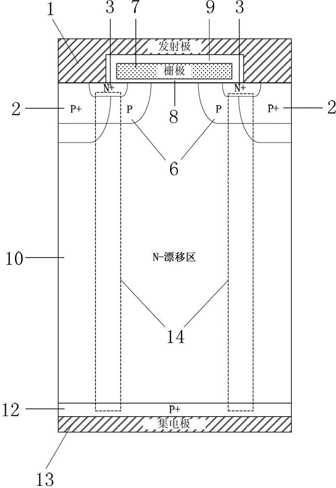
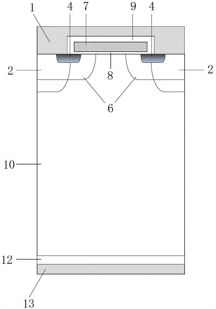
[0023] Anti-latch-up IGBT with variable composition mixed crystal emitter, the structure of which is as Figure 4 As shown, it includes an emitter structure, a collector structure, a gate structure and a drift region structure; the emitter structure includes a metal emitter 1, a P+ ohmic contact region 2, an N+ emitter region 4 and a P-type base region 6, wherein P+ The ohmic contact region 2 and the N+ emitter region 4 are independently located in the P-type base region 6, and the surfaces of the P+ ohmic contact region 2 and the N+ emitter region 4 are all in contact with the metal emitter 1; the collector structure includes a P+ collector Electrical region 12 and metal collector 13, wherein the lower surface of P+ collector region 12 is in contact with metal collector 13; the drift region structure includes N-drift region 10, and the connection between N-drift region 10 and P+ collector region 12 There is a layer of N-type electric field stopping layer 11 between them; the ...
PUM
 Abstract
Description
Claims
Application Information


