
an igbt device

A device and semiconductor technology, applied in the field of power devices, can solve problems such as device reliability

Active Publication Date: 2021-02-12
UNIV OF ELECTRONICS SCI & TECH OF CHINA
View PDF4 Cites 0 Cited by
  • Summary
  • Abstract
  • Description
  • Claims
  • Application Information

AI Technical Summary

Problems solved by technology

[0005] In order to solve the problems caused by the IGBT latch-up effect of the parasitic thyristor in the prior art to the reliability of the device, the present invention provides an IGBT device with high latch-up resistance

Method used


Image

  • an igbt device
  • an igbt device
  • an igbt device

Examples


Embodiment 1

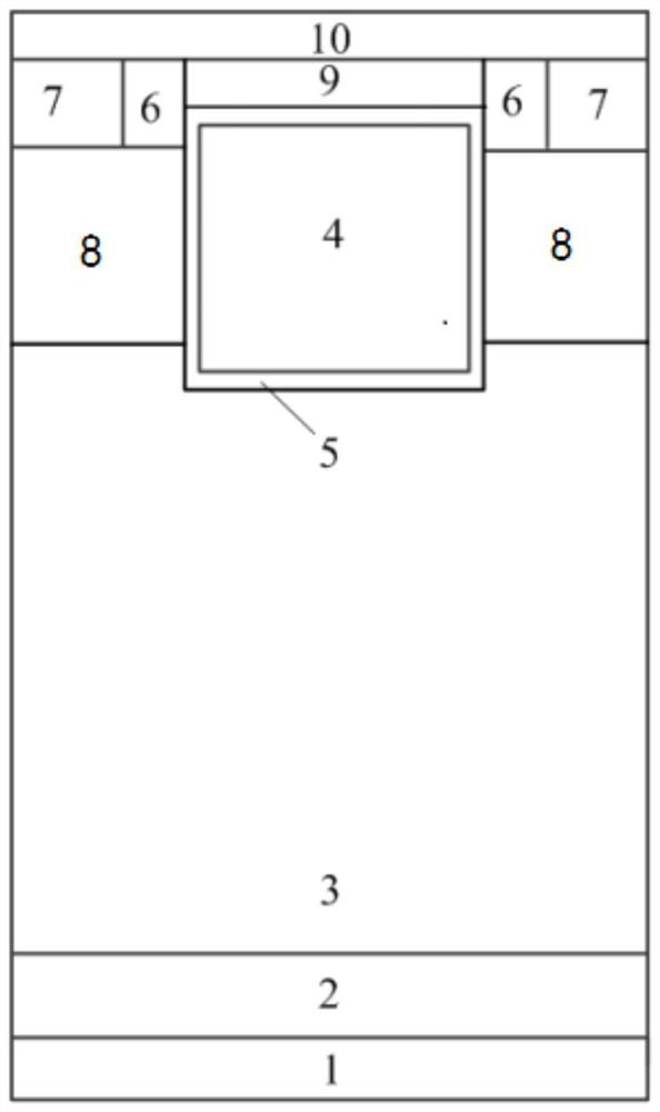
[0020] Such as image 3 As shown, this embodiment provides an insulated gate bipolar transistor (IGBT), including a metallized collector 1, a semiconductor collector region 2 of a first conductivity type, a drift region 3 of a semiconductor of a second conductivity type, a gate structure, a second A conductivity type semiconductor base region 8, a first conductivity type semiconductor contact region 7, a second conductivity type semiconductor emitter region 6 and a metal emitter 10; the metallized collector electrode 1 is located on the back side of the first conductivity type semiconductor collector region 2, the second The second conductivity type semiconductor drift region 3 is located on the front of the first conductivity type semiconductor collector region 2, and the top of the second conductivity type semiconductor drift region 3 is connected to the metal emitter 10; the top layer of the second conductivity type semiconductor drift region 3 is provided with the first A ...

Embodiment 2

[0024] Such as Figure 4As shown, in the present invention, except that the first conductivity type semiconductor base region 8 is composed of several sub-regions with different doping concentrations, assuming that the number of sub-regions is n, then n≥3; n sub-regions satisfy: in the longitudinal direction of the device , as the distance from the metal emitter 10 gradually increases, the doping concentration of each sub-region in the first conductivity type semiconductor base region 8 gradually increases.


PUM


Abstract

The invention provides an IGBT device and belongs to the technical field of power devices. The present invention includes a metallized collector electrode, a first conductivity type semiconductor collector region, a second conductivity type semiconductor drift region and a metal emitter stacked sequentially from bottom to top; the second conductivity type semiconductor drift region has a gate structure and is located The first conductivity type semiconductor base region on both sides of the gate structure, the first conductivity type semiconductor contact region in the first conductivity type semiconductor base region, the second conductivity type semiconductor emission region; and the doping concentration of the first conductivity type semiconductor base region It gradually increases from close to the metal emitter to away from the metal emitter. The present invention reasonably adjusts the doping concentration of the base region so that the concentration near the emitter region is relatively low to form a minority carrier deceleration field in the base region to suppress the occurrence of latch-up, thereby improving the IGBT without affecting the normal operating characteristics of the IGBT. The device's immunity to latch-up.

Description

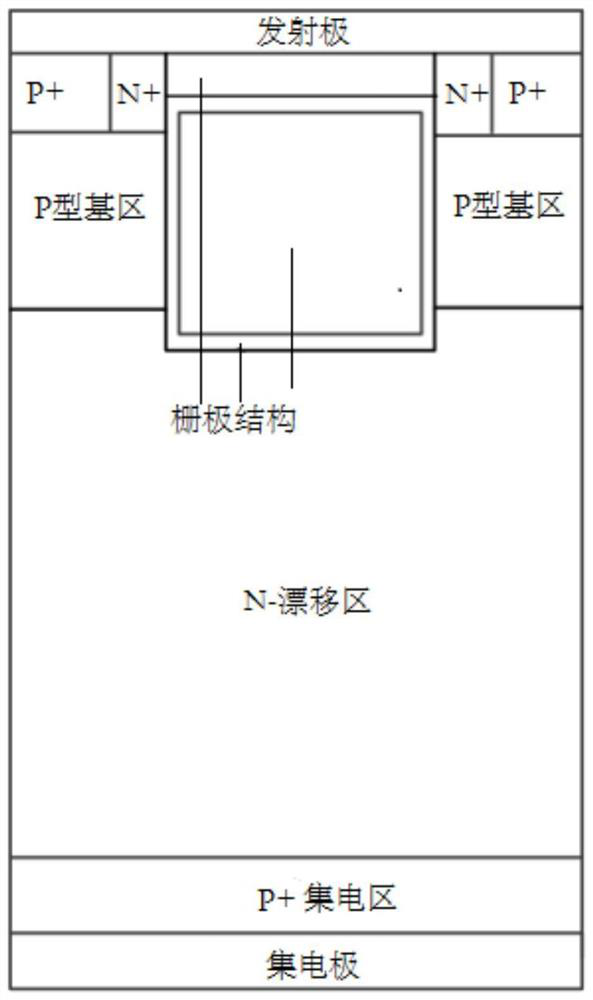
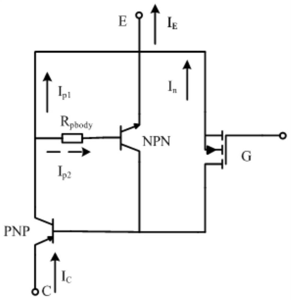
technical field [0001] The invention belongs to the technical field of power devices, in particular to an IGBT device with high latch-up resistance. Background technique [0002] IGBT is a representative type of power semiconductor devices. Because of its advantages of high withstand voltage, low on-resistance, easy driving, and fast switching speed, it is widely used in switching power supplies, frequency conversion speed regulation, inverters, etc. There are important applications in the field of power. However, the latch-up problem is one of the important reasons that threaten the reliability of IGBTs. [0003] Such as figure 1 and figure 2 Shown are the structural schematic diagram and the equivalent circuit of the traditional N-channel IGBT device respectively. Depend on figure 1 It can be seen that the IGBT structure contains the N + Emitter, P-type base, N - drift region and P + The N-P-N-P four-layer tri-crystal thyristor structure composed of the collector ...

Claims


Application Information

Patent Timeline
Patent Type & Authority Patents(China)
IPC IPC(8): H01L29/739H01L29/10
CPCH01L29/1004H01L29/7393H01L29/7395
Inventor 任敏林育赐罗蕾谢驰李佳驹李泽宏张波
Owner UNIV OF ELECTRONICS SCI & TECH OF CHINA
Learn More