

IGBT device
Patent Information
- Authority / Receiving Office
- CN · China
- Current Assignee / Owner
- UNIV OF ELECTRONIC SCI & TECH OF CHINA
- Publication Date
- 2017-12-26
Smart Images
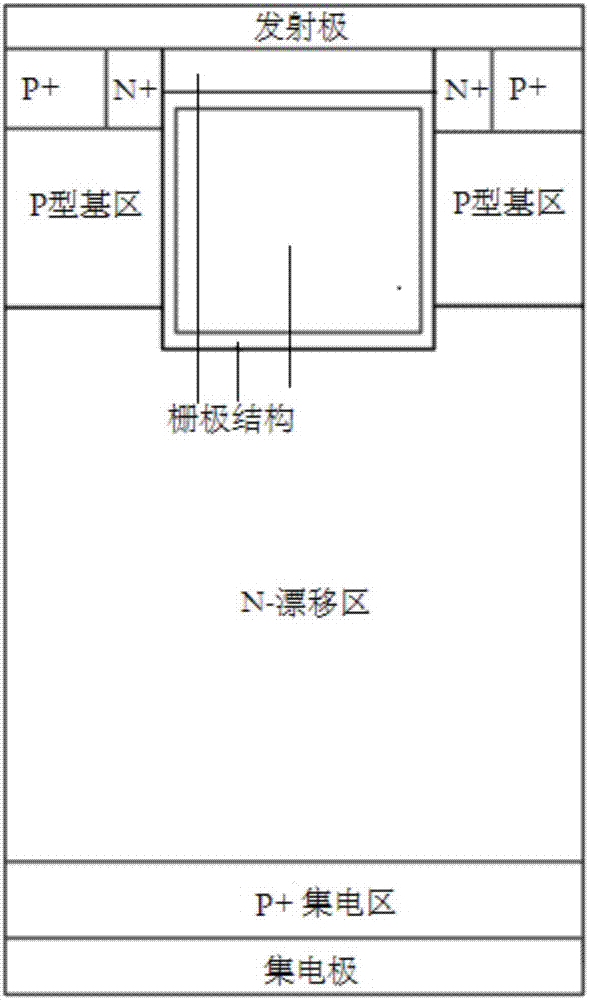
Figure 1 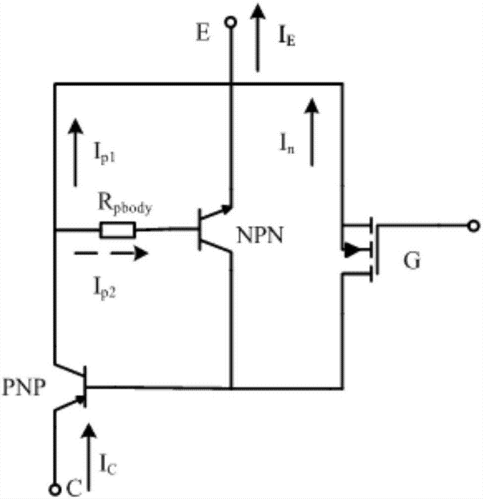
Figure 2 
Figure 3
Abstract
Description
technical field
[0001] The invention belongs to the technical field of power devices, in particular to an IGBT device with high latch-up resistance. Background technique
[0002] IGBT is a representative type of power semiconductor devices. Because of its advantages of high withstand voltage, low on-resistance, easy driving, and fast switching speed, it is widely used in switching power supplies, frequency conversion speed regulation, inverters, etc. There are important applications in the field of power. However, the latch-up problem is one of the important reasons that threaten the reliability of IGBTs.
[0003] Such as figure 1 and figure 2 Shown are the structural schematic diagram and the equivalent circuit of the traditional N-channel IGBT device respectively. Depend on figure 1 It can be seen that the IGBT structure contains the N + Emitter, P-type base, N - drift region and P + The N-P-N-P four-layer tri-crystal thyristor structure composed of the collector ...