Heterjunction bipolar transistor with tunnelling mis emitter junction

A technology for emitters and transistors, which is applied in semiconductor devices, semiconductor/solid-state device manufacturing, electrical components, etc., can solve problems such as unreported passivation materials, improve emitter efficiency, increase electron migration, increase device and circuit products rate effect

Inactive Publication Date: 2006-11-15
埃皮泰克帝斯克有限公司
View PDF0 Cites 0 Cited by
  • Summary
  • Abstract
  • Description
  • Claims
  • Application Information

AI Technical Summary

Problems solved by technology

While silicon dioxide is known to form a good passivation layer on silicon, equivalent passivation materials for compound semiconductors such as gallium arsenide have not been reported for many years

Method used


Image

  • Heterjunction bipolar transistor with tunnelling mis emitter junction
  • Heterjunction bipolar transistor with tunnelling mis emitter junction
  • Heterjunction bipolar transistor with tunnelling mis emitter junction

Examples


Embodiment Construction

[0073] In the following detailed description, reference is made to the accompanying drawings which form a part hereof, and in which is shown by way of illustration a specific preferred embodiment in which the invention may be practiced. These embodiments are described in sufficient detail to enable those skilled in the art to practice the invention, and it is to be understood that other embodiments may be utilized and structural, material and electrical changes may be made without departing from the invention. scope. Accordingly, the following detailed description should not be taken in a limiting sense, and the scope of the present invention is defined only by the appended claims.

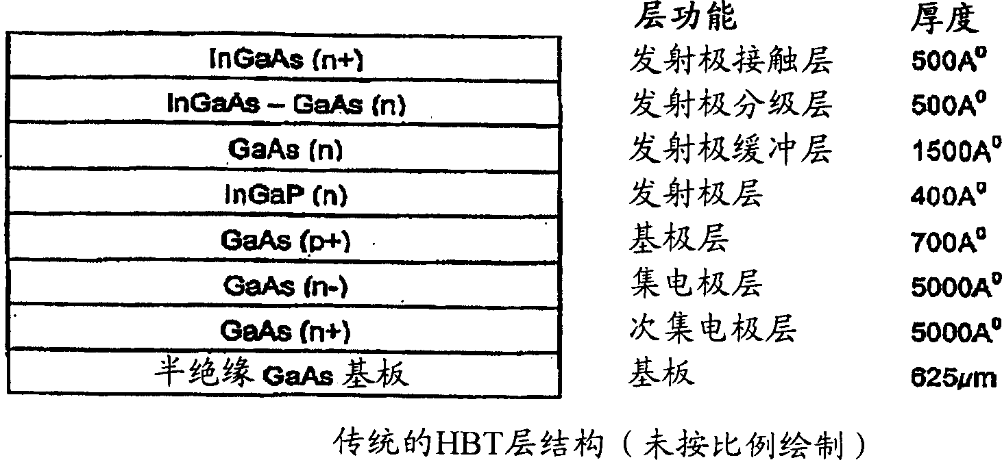
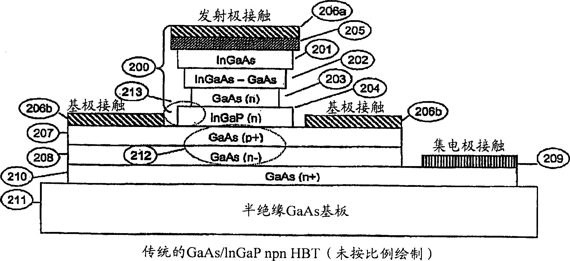
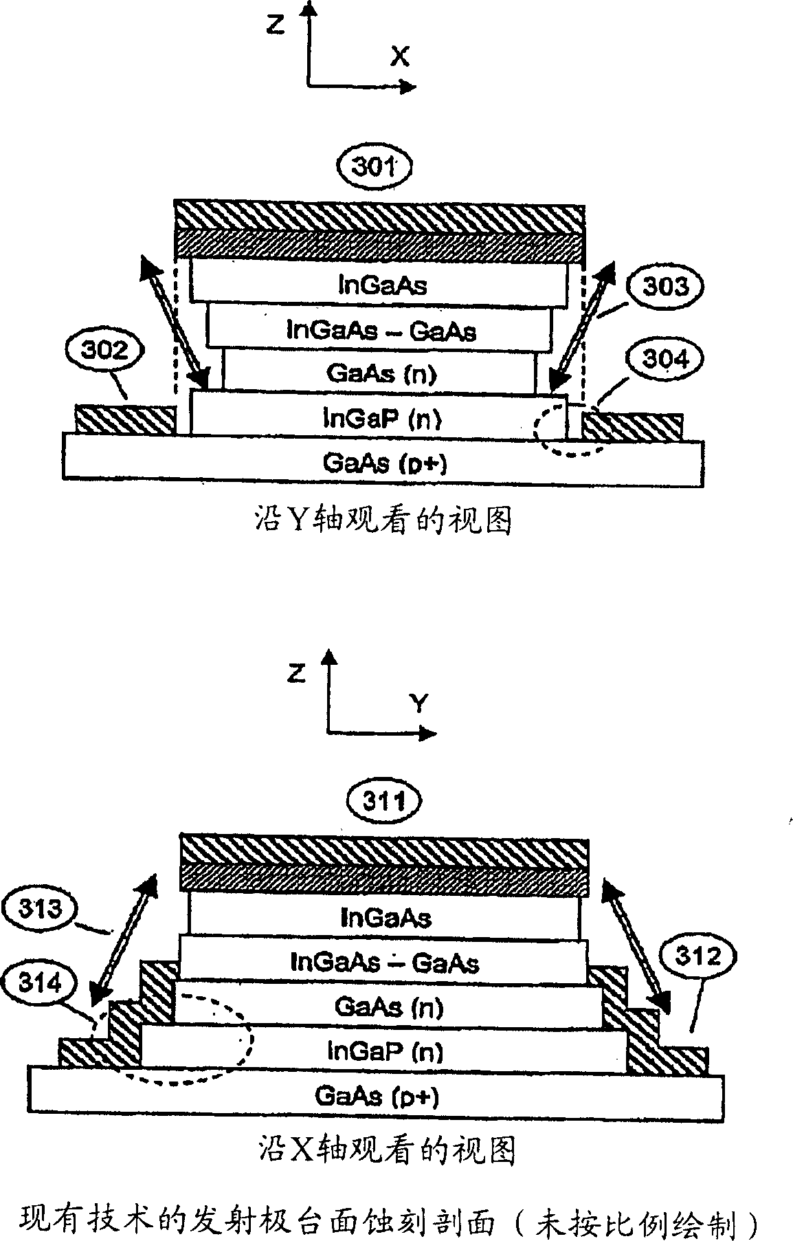
[0074] According to the present invention, improved integrated circuits are provided. More specifically, the present invention provides a method and structure for a high performance heterojunction bipolar transistor suitable for compound semiconductor material systems such as gallium arsenide, an...


PUM


Abstract

A method and structure are provided for a high performance heterojunction bipolar transistor which is suited to compound semiconductor systems such as gallium arsenide (GaAs) and which utilises an emitter junction formed from a plurality of metal layers and a plurality of ultra-thin insulating layers. The metal layers chosen have work functions which form a tunnelling Metal-Insulator-Semiconductor Junction when deposited on top of an ultra-thin insulating layer. The insulating layer may be made from a rare-earth oxide such as gadolinium oxide (Gd2O3) which is epitaxially grown on a compound semiconductor substrate and possibly covered with a second ultra-thin insulating layer.

Description

technical field [0001] The present invention generally relates to integrated circuits. More specifically, the present invention provides a fabrication method and structure for a metal-insulator-semiconductor (MIS) transistor structure including compound semiconductor materials. However, it should be understood that many variations, changes and substitutions are possible. It will be convenient to describe the invention hereinafter in relation to a MIS heterojunction bipolar transistor (HBT) comprising a GaAs substrate, however, it should be understood that the invention is not limited to this use. Background technique [0002] The present invention has identified the following background of the invention and related art. Over the years, device designers have recognized the importance of bandgap engineering techniques in designing transistor devices (devices) for high performance applications. As known in the art, bandgap engineering is the technique of fabricating semicond...

Claims


Application Information

Patent Timeline
Patent Type & Authority Applications(China)
IPC IPC(8): H01L29/737H01L21/331
CPCH01L29/0817H01L29/0895H01L29/66318H01L29/7311H01L29/7371
Inventor 肖恩·约瑟夫·坎宁安
Owner 埃皮泰克帝斯克有限公司
Why Eureka
Try Eureka