Semiconductor chip test baseboard

A chip testing and semiconductor technology, applied in the direction of measuring devices, measuring device casings, measuring instrument components, etc., can solve the problems that the chip cannot be pressed down correctly, cannot meet the test requirements, cannot realize position adjustment, etc., and can expand the position adjustment range, The effect of meeting test requirements and improving positioning accuracy

Inactive Publication Date: 2013-12-18
ACETEC SEMICON
View PDF10 Cites 0 Cited by
  • Summary
  • Abstract
  • Description
  • Claims
  • Application Information

AI Technical Summary

Problems solved by technology

However, when the test base plate is fixed relative to the test base, it only plays a role of coarse adjustment, so the two positioning holes on it cannot realize position adjustment
Due to machining errors, sometimes it is impossible to meet the test requirements only by adjusting the position of the test base, that is, the chip cannot be correctly pressed into the socket of the test board.

Method used


Image

  • Semiconductor chip test baseboard
  • Semiconductor chip test baseboard

Examples


Embodiment 1

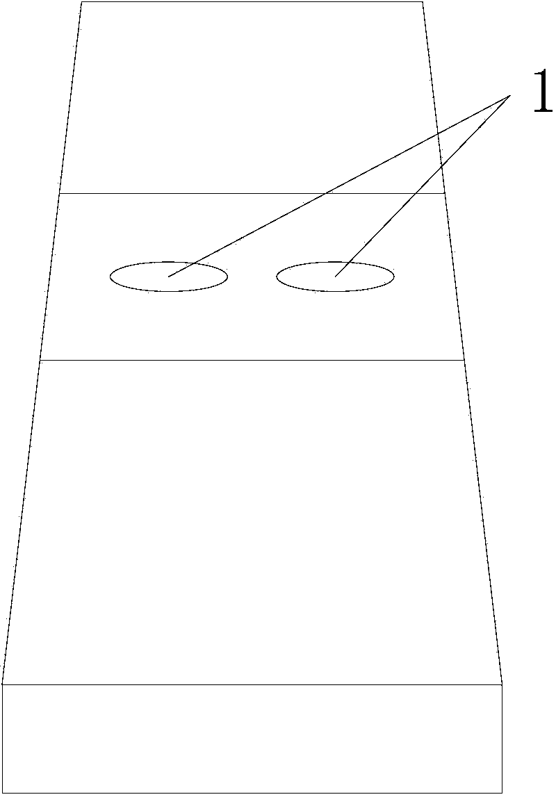
[0011] Embodiment 1: as attached figure 1 As shown, a semiconductor chip test base plate is provided with two positioning holes 1 on it. The shape of the positioning holes 1 is elliptical. The angular direction of the ellipse opening should be consistent.

[0012] When the test base plate is fixed on the test base, the positioning is roughly adjusted relative to the test base, and then finely adjusted and positioned through the test base to meet the test requirements, ensure that the chip is correctly pressed into the socket, protect the socket, and improve the test yield .

Embodiment 2

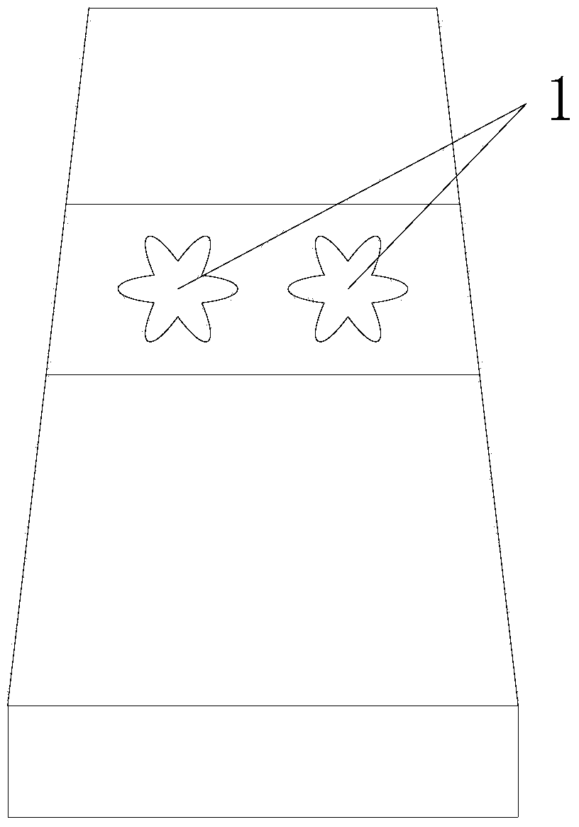
[0013] Embodiment 2: basically the same as Embodiment 1, the difference is: as attached figure 2 As shown, each positioning hole 1 is formed by a group of ellipses with the same center, and is opened radially from the center point, providing adjustment space in multiple directions for the position adjustment of the test base plate. A group of each positioning hole 1 The ovals are the same size.


PUM


Abstract

The invention discloses a semiconductor chip test baseboard. A positioning hole is formed in the semiconductor chip test baseboard and is oval. The semiconductor chip test baseboard has the advantages that the positioning hole formed in a test base board is improved, so that the test base board has a certain position adjusting range relative to a test base, the adjusting directions are not single, the position adjusting range of a test device is widened, the positioning accuracy is improved, a chip is ensured to be correctly pressed into a socket, and the test requirements are met.

Description

technical field [0001] The invention relates to a testing device in the semiconductor testing industry, in particular to a semiconductor chip testing bottom plate. Background technique [0002] In the existing semiconductor chip testing device, the test board is fixed on the test base plate, and the test base plate is then fixed on the test base. The test base can be adjusted from left to right, front to back, and plays a fine-tuning role. However, when the test base plate is fixed relative to the test base, it only plays a rough adjustment role, so the two positioning holes on it cannot realize position adjustment. Due to errors in machining, sometimes the test requirements cannot be met only by adjusting the position of the test base, that is, the chip cannot be correctly pressed into the socket of the test board. Contents of the invention [0003] Object of the invention: In view of the above problems, the object of the invention is to provide a semiconductor chip tes...

Claims


Application Information

Patent Timeline
Patent Type & Authority Applications(China)
IPC IPC(8): G01D11/00G01R1/04
Inventor 王刚毛丹辉
Owner ACETEC SEMICON
Why Eureka
Try Eureka