Array substrate and manufacturing method thereof and 3D (three-dimensional) display device

A technology of an array substrate and a manufacturing method, which is applied in the field of 3D display, and can solve problems such as difficulty in alignment and lamination of a grating substrate and a display screen, inability to improve the brightness of a display device, and low yield rate, etc.

Inactive Publication Date: 2013-12-18
BOE TECH GRP CO LTD
View PDF5 Cites 47 Cited by
  • Summary
  • Abstract
  • Description
  • Claims
  • Application Information

AI Technical Summary

Problems solved by technology

[0004] (1) Due to the addition of the grating substrate, the transmittance of light is low, and the brightness of the display device is low. At the same time, due to the existence of the grating substrate, the overall thickness of the display device increases;
[0005] (2) The grating area needs to be aligned with the pixel area. In the manufacturing process, it is difficult to align the grating substrate with the grating layer and the display screen, and the yield rate is low. At the same time, the pixel alignment accuracy of the grating and the array substrate is also low. It will greatly affect the display

Method used


Image

  • Array substrate and manufacturing method thereof and 3D (three-dimensional) display device
  • Array substrate and manufacturing method thereof and 3D (three-dimensional) display device
  • Array substrate and manufacturing method thereof and 3D (three-dimensional) display device

Examples


Embodiment 1

[0050] The array substrate provided by this embodiment is as Figure 4As shown, it includes: a base substrate 100 (a glass substrate or a transparent substrate of quartz material) and a pixel array layer 200 located above the base substrate 100, and also includes: a number of baffles located below the base substrate 100 with predetermined distances The grating layer formed by the light stripes.

[0051] In this embodiment, the light-shielding strip includes: a light-shielding layer 410 and a light-reflecting layer 420 , and the light-shielding layer 410 is located between the base substrate 100 and the light-reflecting layer 420 . To achieve a better 3D display viewing angle, the width and spacing of the light-shielding strips have been set in advance. In order not to affect the 3D display viewing angle, the projection of the light-reflecting layer 420 on the base substrate 100 is projected by the light-shielded layer 410 on the base substrate 100. projection overlay on .

...

Embodiment 2

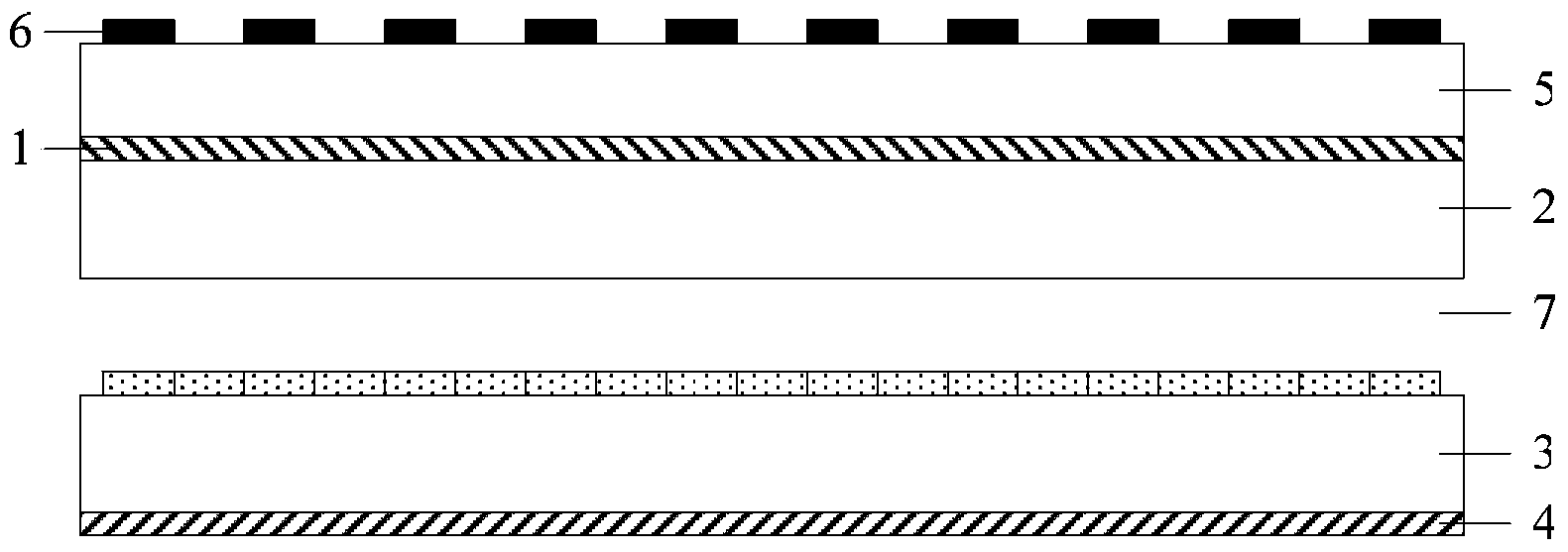
[0062] For a liquid crystal display device, a lower polarizer is required under the base substrate 100 . Therefore, on the basis of Embodiment 1, the array substrate of this embodiment further includes a polarizer formed on the side of the light blocking strip away from the pixel array layer. Such as Figure 5 As shown, the polarizer 300 is formed under the reflective layer 420 . During fabrication, the polarizer 300 is directly formed under the reflective layer 420 on the basis of the fabrication process in Embodiment 1. It is only necessary to ensure that the reflective layer 420 is formed before manufacturing the polarizer 300 .

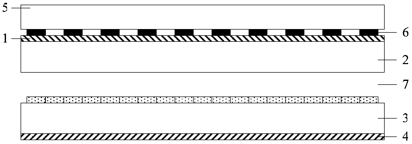
[0063] Of course, if Figure 6 As shown, the polarizer 300 can also be formed between the light-shielding layer 410 of the light-shielding strip and the base substrate 100, that is, the light-shielding layer 410 is directly formed on the lower surface of the polarizer 300, and the light-reflecting layer 420 is formed on the lower surface of the ...

Embodiment 3

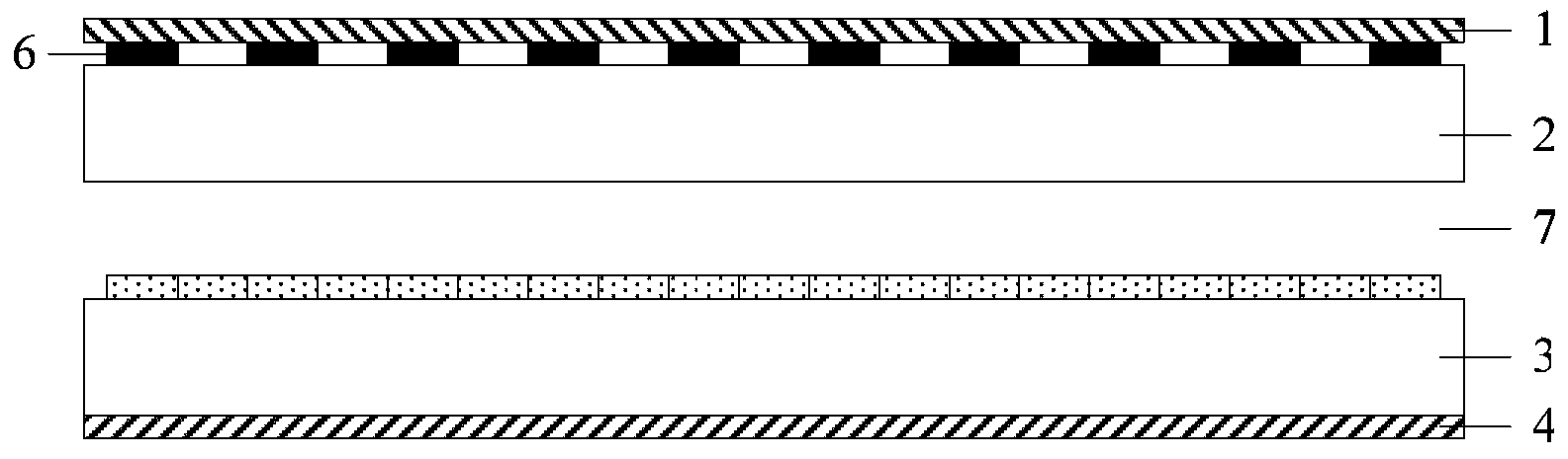
[0074] The array substrate of this embodiment is such as Figure 7 As shown, it includes: a base substrate 100 (a glass substrate or a transparent substrate of quartz material) and a pixel array layer 200 located above the base substrate 100, and also includes: a number of baffles located below the base substrate 100 with predetermined distances The grating layer formed by the light strip 400'.

[0075] In this embodiment, the light blocking strip 400' is made of reflective material. Preferably, the light blocking strip 400 ′ is directly formed on the lower surface of the base substrate 100 , so that the grating substrate is not needed, and the transmittance of light is increased. When directly formed, the light blocking strip 400 ′ is formed on the lower surface of the base substrate 100 by a patterning process (usually including processes such as photoresist coating, exposure, development, etching, and photoresist stripping). , improving the alignment accuracy of the sub-p...


PUM


Abstract

The invention relates to the technical field of display and discloses an array substrate. The array substrate comprises a substrate and a pixel array layer located on the substrate, and also comprises a grating layer which is formed by a plurality of light blocking strips spaced at a preset distance and is used for 3D display. The grating layer is located at one side of the pixel array layer, which is back on to the substrate, or located at one side of the substrate, which faces the pixel array layer, or located at one side of the substrate, which is back on to the pixel array layer; the light blocking strips are used for reflecting light rays irradiated to the pixel array layer through the substrate. According to the array substrate disclosed by the invention, the grating layer is arranged at one side of the array substrate, which is back on to the pixel array layer, and the light blocking strips of the grating layer can be used for reflecting the light rays irradiated to the pixel array layer through the substrate. When display is performed, the light which is emitted from a backlight source and does not transmit the grating layer is reflected to the backlight source, and as the backlight source is usually provided with a light guide plate for the light to be diffused, and the light reflected to the backlight source is reflected again by the light guide plate to transmit the grating layer, the display brightness is improved.

Description

technical field [0001] The present invention relates to the technical field of 3D display, in particular to an array substrate, a manufacturing method thereof, and a 3D display device. Background technique [0002] At present, the relatively mature grating naked-eye 3D technology has a basic structure of attaching a grating layer outside the upper polarizer of the display screen, through which the light emitted by the pixels in the display screen is respectively output to the left and right eyes of the viewer. , resulting in a stereoscopic effect. The structure of the existing naked-eye 3D display device is as follows: figure 1 and figure 2 as shown, figure 1 The display device shown in includes a display screen formed by an upper polarizer 1 positioned above a color filter substrate 2, a lower polarizer 4 positioned below an array substrate, and a pair of a color filter substrate 2 and an array substrate 3. The color filter substrate 2 Between the liquid crystal layer ...

Claims


Application Information

Patent Timeline
IPC IPC(8): G02F1/1335G02F1/1362G02B27/26G02B30/25
CPCG02F1/133512G02B30/25
Inventor 魏伟武延兵
Owner BOE TECH GRP CO LTD
Why Eureka
Try Eureka