pixel structure
A technology of pixel structure and pixel area, applied in the direction of optical components, optics, instruments, etc., can solve the problem of poor color of electrowetting display technology, and achieve the effect of improving color shift phenomenon
- Summary
- Abstract
- Description
- Claims
- Application Information
AI Technical Summary
Problems solved by technology
Method used
Image
Examples
Embodiment Construction
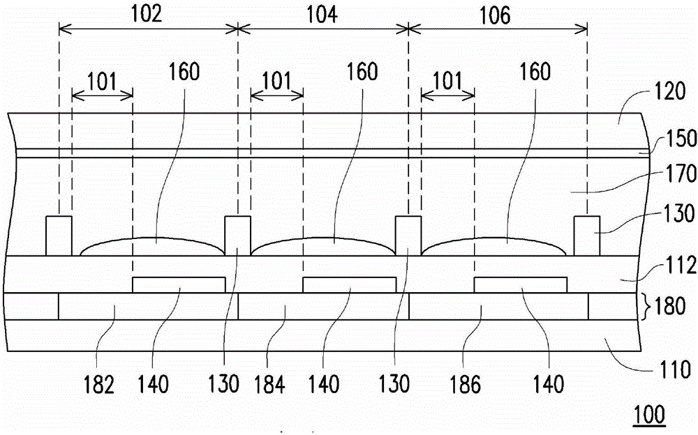
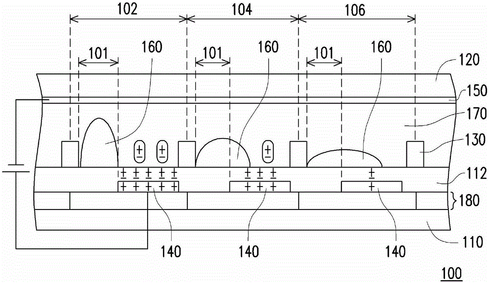
[0050] Figure 1A To show a cross-sectional view of a pixel structure 100 according to an experimental example of the present invention, and Figure 1B to show Figure 1A A cross-sectional view of the pixel structure 100 when a bias voltage is applied. Please refer to Figure 1A and 1B , The pixel structure 100 includes a first substrate 110, a second substrate 120, a plurality of partition walls 130, a plurality of pixel electrodes 140, a common electrode 150, a plurality of colored display media 160, a light-transmitting display media 170 and a color filter layer 180 . In addition, the pixel structure 100 may have a plurality of sub-pixel regions 102 , 104 and 106 .
[0051]The first substrate 110 and the second substrate 120 are spaced apart from each other. A film layer 112 is disposed on the first substrate 110 , and the film layer 112 faces the second substrate 120 . The partition wall 130 is disposed on the film layer 112 , and the partition wall 130 is located betw...
PUM
 Abstract
Description
Claims
Application Information


