OLED substrate and manufacturing method thereof, and display device

A manufacturing method and substrate technology, applied in the direction of final product manufacturing, sustainable manufacturing/processing, climate sustainability, etc., can solve problems such as easy color shift of images, redness of displayed images, poor display effect of AMOLED panels, etc. Achieve the effect of ensuring display effect and improving OLED color cast

Active Publication Date: 2018-10-23
BOE TECH GRP CO LTD +1
View PDF12 Cites 19 Cited by
  • Summary
  • Abstract
  • Description
  • Claims
  • Application Information

AI Technical Summary

Problems solved by technology

However, after long-term use of the AMOLED panel produced by the FFM process, the image displayed by the AMOLED panel is particularly prone to color shift, such as redness of the displayed image, resulting in poor display effect of the AMOLED panel

Method used


Image

  • OLED substrate and manufacturing method thereof, and display device
  • OLED substrate and manufacturing method thereof, and display device
  • OLED substrate and manufacturing method thereof, and display device

Examples


Embodiment Construction

[0026] In order to further illustrate the OLED substrate, manufacturing method, and display device provided by the embodiments of the present invention, a detailed description will be given below in conjunction with the accompanying drawings.

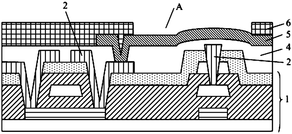
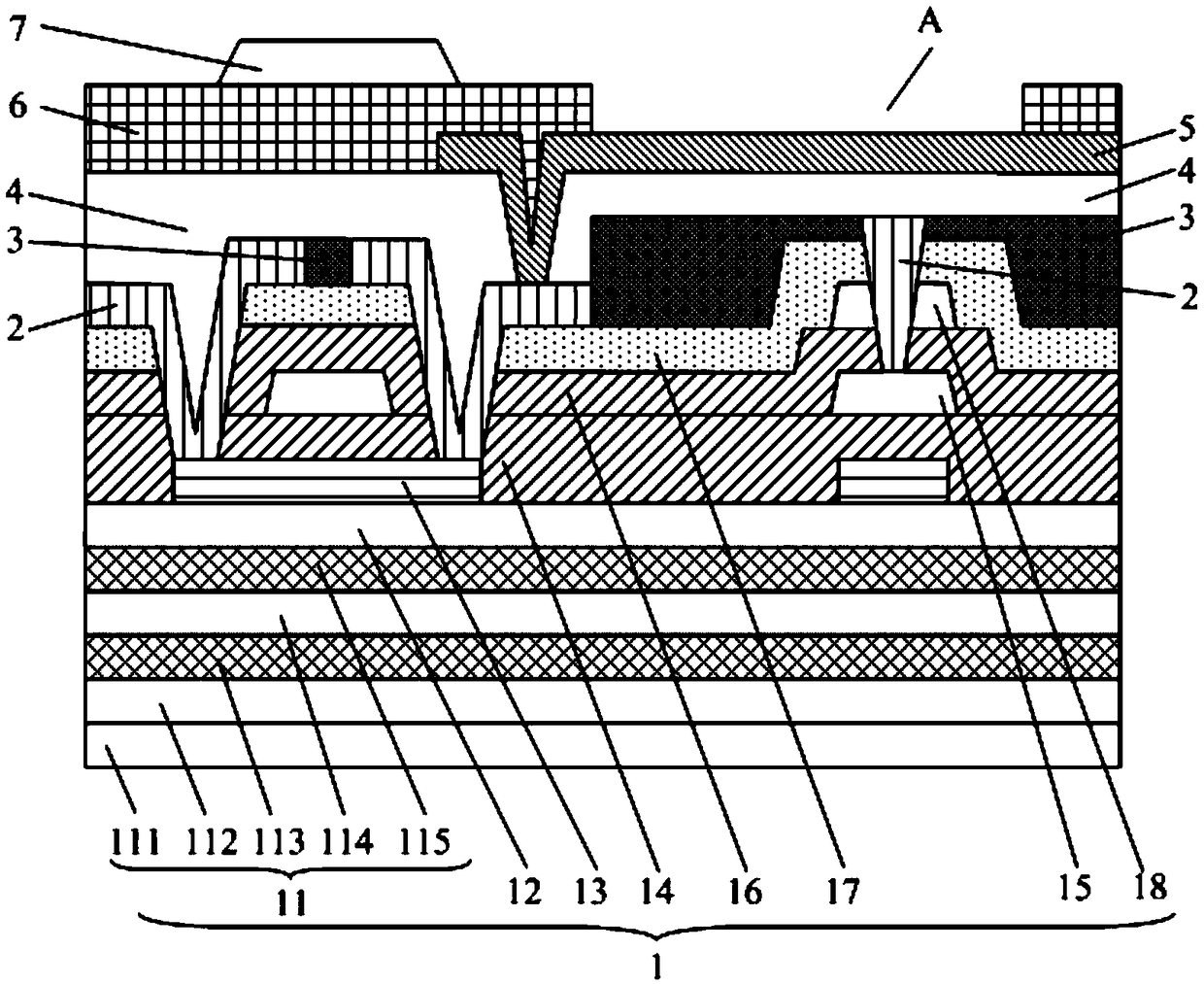
[0027] see figure 1 , a common OLED substrate includes a base substrate 1 and a metal wiring 2 fabricated on the surface of the base substrate 1 by FFM technology; the surface of the base substrate 1 not covered by the metal wiring 2 and the metal wiring 2 facing away from the base substrate 1 is formed with a planarization layer 4, and the surface of the planarization layer 4 facing away from the base substrate 1 is respectively formed with an OLED anode 5 and a pixel defining layer 6, and the area of ​​the pixel defining layer 6 opposite to the OLED anode 5 is provided with a pixel hole A .

[0028] However, since the bottom of the pixel hole A in the OLED substrate, that is, the bottom of the OLED anode 5 is inevitably formed with a...


PUM


Abstract

The embodiment of the invention, which relates to the technical field of display, discloses an OLED substrate and a manufacturing method thereof, and a display device so that a problem of OLED color casting in the existing OLED display device can be solved. The OLED substrate comprises a substrate; a patterned metal routing part is formed on the surface of the substrate; a flatness adjusting layeris formed on the surface, not being covered by the metal routing part, of the substrate; a planarization layer is formed on the surface, in opposite to the substrate, of the flatness adjusting layerand the surface, in opposite to the substrate, of the metal routing part; and an OLED anode is formed on the surface, in opposite to the substrate, of the planarization layer. The metal routing part and the flatness adjusting layer are formed by using a same mask respectively. The provided OLED substrate is used for AMOLED displaying.

Description

technical field [0001] The invention relates to the field of display technology, in particular to an OLED substrate, a manufacturing method, and a display device. Background technique [0002] Active-matrix organic light emitting diode (AMOLED) panels are widely used in the display field due to their advantages of high brightness, full viewing angle, fast response speed, and flexible display. [0003] At present, in the process of making small-sized AMOLED panels, the Fine Metal Mask (FFM) process is mostly used to make the metal traces on the Low Temperature Poly-Silicon (LTPS) backplane of the AMOLED panel. Wire. However, after long-term use of the AMOLED panel produced by the FFM process, the image displayed by the AMOLED panel is particularly prone to color shift, such as reddish display image, resulting in poor display effect of the AMOLED panel. Contents of the invention [0004] The purpose of the embodiments of the present invention is to provide an OLED substrat...

Claims


Application Information

Patent Timeline
Patent Type & Authority Applications(China)
IPC IPC(8): H01L27/32
CPCH10K59/12H10K59/1201Y02E10/549Y02P70/50H10K59/124H10K59/131H10K77/111H10K59/122H10K71/00
Inventor 吴奕昊辛燕霞于名印包征李博李雪萍
Owner BOE TECH GRP CO LTD
Why Eureka
Try Eureka