Flexible array substrate and manufacturing method thereof

A technology of flexible array and manufacturing method, which is applied in semiconductor/solid-state device manufacturing, electrical components, electric solid-state devices, etc., and can solve problems such as irreparable film layers, increased stress of inorganic film layers, and affecting the display effect of flexible display devices. To achieve the effect of guaranteeing the display effect

Active Publication Date: 2018-04-20
WUHAN CHINA STAR OPTOELECTRONICS SEMICON DISPLAY TECH CO LTD
View PDF3 Cites 29 Cited by
  • Summary
  • Abstract
  • Description
  • Claims
  • Application Information

AI Technical Summary

Problems solved by technology

[0005] The present invention provides a flexible array substrate and its manufacturing method to solve the problem that when the current flexible display device is bent, the stress of the inorganic film layer of the flexib

Method used


Image

  • Flexible array substrate and manufacturing method thereof
  • Flexible array substrate and manufacturing method thereof
  • Flexible array substrate and manufacturing method thereof

Examples


Embodiment 1

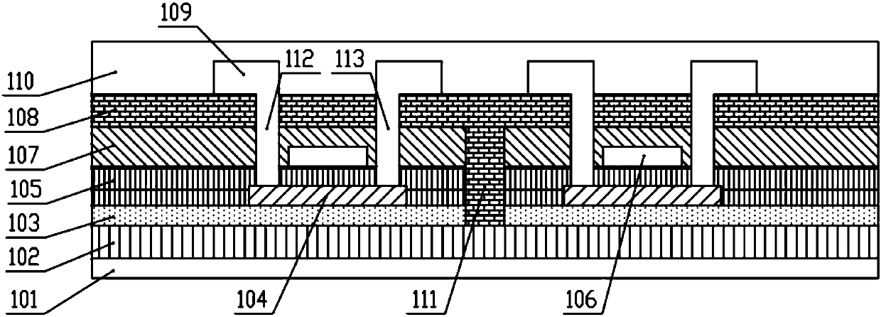
[0059] figure 1 It is a film structure diagram of a flexible array substrate according to a preferred embodiment of the present invention. The flexible array substrate includes: a glass substrate 101, a flexible substrate substrate 102, a buffer layer 103, an active layer 104, a gate insulating layer 105, a second A metal layer 106 , an insulating layer 107 , a flexible organic layer 108 , a second metal layer 109 and a passivation layer 110 .

[0060] The flexible base substrate 102, that is, a polyimide film, is formed on the surface of the glass substrate 101 as the base of the flexible display panel;

[0061] The polyimide film is the film insulation material with the best performance in the world, and has strong tensile strength. It is made of pyromellitic dianhydride and diaminodiphenyl ether through polycondensation and It is cast into a film and then imidized.

[0062] The buffer layer is disposed on the surface of the flexible substrate 102, and the active layer 104...

Embodiment 2

[0074] Figure 5 It is a film structure diagram of a flexible array substrate according to the preferred embodiment 2 of the present invention. The flexible array substrate includes: a glass substrate 201, a flexible substrate substrate 202, a buffer layer 203, an active layer 204, a gate insulating layer 205, a second A metal layer 206 , an insulating layer 207 , a flexible organic layer 208 , a second metal layer 209 and a passivation layer 210 .

[0075] The difference from Embodiment 1 is that the flexible organic layer 208 is formed on the surface of the inter-insulating layer 207, and the flexible organic layer 208 is processed by patterning the flexible organic material deposited on the surface of the inter-insulating layer 207. , formed by retaining at least a part of the flexible organic material that has been patterned;

[0076] The second metal layer 209 is formed on the surface of the inter-insulating layer 207, the second metal layer 209 is patterned to form the ...

Embodiment 3

[0080] Figure 6 It is a flowchart of steps of a method for manufacturing a flexible array substrate in a preferred embodiment, Figure 7 Shown is a process completion diagram of a method for manufacturing a flexible array substrate according to Embodiment 3 of the present invention. The method includes:

[0081] In step S10 , a glass substrate is provided, and the flexible substrate 302 , the buffer layer 303 , the active layer 304 and the gate insulating layer 305 are sequentially deposited on the glass substrate.

[0082] Provide a glass substrate, first deposit a flexible substrate substrate 302 on the glass substrate, that is, a polyimide film, formed on the surface of the glass substrate, as the base of the flexible display panel;

[0083] The polyimide film is the film insulation material with the best performance in the world, and has strong tensile strength. It is made of pyromellitic dianhydride and diaminodiphenyl ether through polycondensation and It is cast into...


PUM

PropertyMeasurementUnit
Film thicknessaaaaaaaaaa

Abstract

The invention provides a flexible array substrate and a manufacturing method thereof. The array substrate comprises a glass substrate, a flexible substrate, a buffer layer, an active layer, a gate insulation layer, a first metal layer, an interlayer insulating layer, a flexible organic layer, a second metal layer and a passivation layer, the flexible organic layer comprises at least two first viaholes, and the first via holes penetrate through the interlayer insulating layer, the gate insulation layer and the buffer layer in sequence. The beneficial effects of the flexible array substrate andthe manufacturing method thereof are that the continuous first via holes are arranged between adjacent film transistors, and the first via holes are filled with flexible organic materials so that a flexible display panel has higher bending resistance, and the display effect of the flexible display panel with small radius of curvature is guaranteed.

Description

technical field [0001] The invention relates to the field of display panel manufacturing, in particular to a flexible array substrate and a manufacturing method thereof. Background technique [0002] With the continuous development of display technology, researchers have developed flexible display devices that can be folded or rolled up. Compared with traditional rigid display devices (that is, display devices made on inflexible substrates such as glass), flexible display devices The device has many advantages, such as light weight, small size, more convenient to carry; higher impact resistance and stronger earthquake resistance. With the continuous development of display technology, flexible display devices are more and more used in the field of curved surface display and wearable display due to their own bendable and foldable characteristics. Therefore, they have also become a hot spot in the display field in recent years. . [0003] A flexible display panel, also known ...

Claims


Application Information

Patent Timeline
IPC IPC(8): H01L23/00H01L27/12H01L21/84
CPCH01L23/562H01L27/1218H01L27/1262
Inventor 胡俊艳
Owner WUHAN CHINA STAR OPTOELECTRONICS SEMICON DISPLAY TECH CO LTD
Why Eureka
Try Eureka