Display panel, manufacturing method thereof and display device

A display panel and display area technology, which is applied to static indicators, instruments, nonlinear optics, etc., can solve the problems of long development cycle and difficult realization of sealing materials, and achieve the effect of improving peripheral defects and preventing display abnormalities

Inactive Publication Date: 2014-01-08
BEIJING BOE OPTOELECTRONCIS TECH CO LTD
View PDF3 Cites 4 Cited by
  • Summary
  • Abstract
  • Description
  • Claims
  • Application Information

AI Technical Summary

Problems solved by technology

The inventor believes that the existing improved method has the following shortcomings: first, the contact between the uncured frame sealant and the liquid crystal cannot be avoided at the current level of technology, especially for small-sized products, which is more difficult to achieve; secondly, the material of the sealant The development cycle is long, and other advantages of the material may be sacrificed

Method used


Image

  • Display panel, manufacturing method thereof and display device
  • Display panel, manufacturing method thereof and display device
  • Display panel, manufacturing method thereof and display device

Examples


Embodiment 1

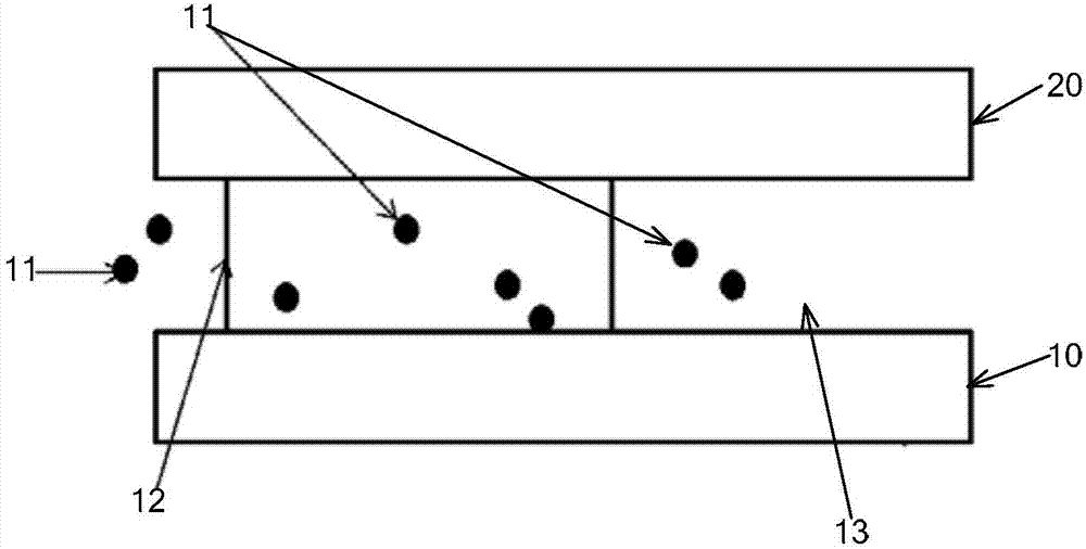
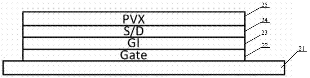
[0045] Most of the sealing glue coating areas around the existing display products are control switches. The specific structure is as follows: figure 2 As shown, it includes: a substrate 21 , a gate metal (Gate) layer 22 , a gate insulating layer (GI) 23 , a source-drain metal (S / D) layer 24 and a passivation layer (PVX) 25 located on the substrate 21 in sequence. Wherein, the gate metal layer 22 and the source-drain metal layer 24 are connected and conducted through a gate insulating layer via hole (GI via hole), serving as a control switch of the peripheral circuit.

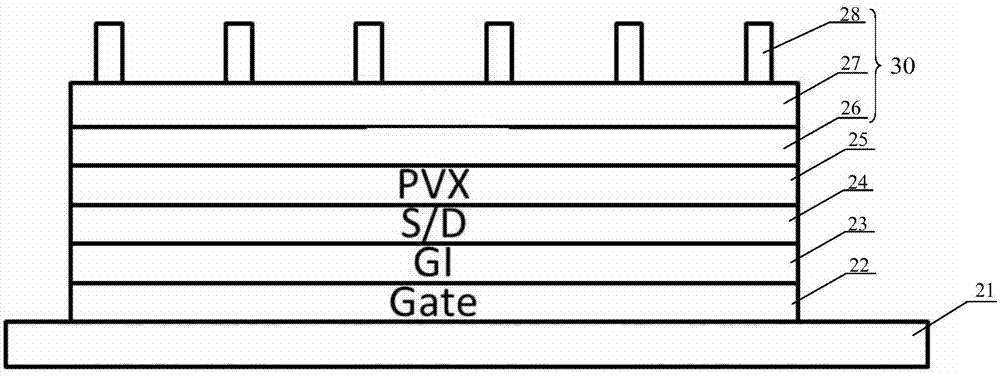
[0046] An embodiment of the present invention provides a display panel. The peripheral area of ​​the display panel is provided with: a dust-proof structure 30; the dust-proof structure 30 is located outside the display area on the display panel and inside the outer edge of the sealant coating area; refer to image 3 As shown, the dustproof structure 30 includes: a first electrode 26, a second electrode 28, and...

Embodiment 2

[0063] On the other hand, an embodiment of the present invention also provides a method for manufacturing a display panel, including: a color filter substrate manufacturing process, an array substrate manufacturing process, and a color filter substrate and array substrate box-to-box manufacturing process, such as Figure 7 As shown, the array substrate manufacturing process includes:

[0064] 101. Forming a gate metal layer, a gate insulating layer, a source-drain metal layer, and a passivation layer sequentially on the substrate;

[0065] 102. On the substrate on which the gate metal layer, gate insulating layer, source-drain metal layer, and passivation layer are formed, form a first transparent conductive film, and form a pixel electrode or a common electrode in a predetermined display area through a patterning process, in the A first electrode is formed between the outside of the preset display area and the inside of the outer edge of the preset sealant application area; ...


PUM

PropertyMeasurementUnit
thicknessaaaaaaaaaa
thicknessaaaaaaaaaa
thicknessaaaaaaaaaa

Abstract

The embodiment of the invention discloses a display panel, a manufacturing method thereof and a display device, and relates to the field of display. The display panel, the manufacturing method thereof and the display device can prevent foreign ions in the external world or in frame sealing glue from entering a display area, and thus poor periphery of a displayer can be overcome. A dustproof structure is arranged on the periphery area of the display panel, the dustproof structure is located on the outer side of the display area of the display panel and on the inner side of the outer edge of a frame sealing glue coating area, the dustproof structure comprises first electrodes, second electrodes and an insulating layer sandwiched between the first electrodes and the second electrodes, and slots are formed in the second electrodes.

Description

technical field [0001] The invention relates to the display field, in particular to a display panel, a manufacturing method thereof, and a display device. Background technique [0002] The panel molding process is a relatively important step in the production process of liquid crystal displays. It is mainly to pour the array substrate 10 and the color filter substrate 20 produced in the previous process into liquid crystal after alignment treatment and alignment bonding. figure 1 As shown, in this process, the external environment or impurity ions 11 in the sealant 12 will often enter the peripheral display area 13, causing the liquid crystal in the peripheral display area 13 to be polluted, which will easily lead to peripheral defects of the liquid crystal display. [0003] The existing improvement methods are generally divided into two categories: first, from the process, try to reduce the contact time between the uncured sealant and the liquid crystal, thereby reducing th...

Claims


Application Information

Patent Timeline
Patent Type & Authority Applications(China)
IPC IPC(8): G02F1/1339G02F1/1333
CPCG02F1/133308G09G3/3611G09G2330/04G09G2300/0426G02F1/133311G09G3/3648
Inventor 肖昂
Owner BEIJING BOE OPTOELECTRONCIS TECH CO LTD
Why Eureka
Try Eureka