nmos transistor and its formation method, sram memory cell circuit

A technology of transistors and semiconductors, applied in the direction of transistors, circuits, electrical components, etc., can solve problems such as increased threshold voltage changes and lower operating voltages, and achieve the effects of improving write margins and improving read and write stability

Active Publication Date: 2016-01-06
SEMICON MFG INT (SHANGHAI) CORP
View PDF4 Cites 0 Cited by
  • Summary
  • Abstract
  • Description
  • Claims
  • Application Information

AI Technical Summary

Problems solved by technology

[0010] However, as the process node of the CMOS process decreases, the operating voltage decreases, and random doping leads to an increase in threshold voltage variation, which poses challenges to the read stability of SRAM.

Method used


Image

  • nmos transistor and its formation method, sram memory cell circuit
  • nmos transistor and its formation method, sram memory cell circuit
  • nmos transistor and its formation method, sram memory cell circuit

Examples


Embodiment Construction

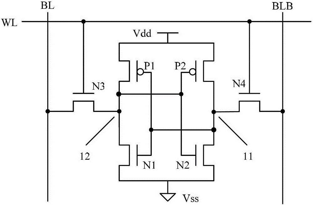
[0038] The read and write stability of SRAM memory is mainly measured by the two parameters of read margin and write margin. The read margin is the maximum noise voltage that the SRAM memory can withstand without changing the storage state during the read operation. , the write margin is the maximum noise voltage that the SRAM memory can withstand without changing the storage state during the write operation. The higher the read margin and the write margin, the better the read and write stability of the SRAM memory. Among them, the read margin is related to the ratio between the saturated source-drain current value of the pull-down NMOS transistor and the saturated source-drain current value of the pass NMOS transistor; the write margin is related to the saturated source-drain current value of the pass NMOS transistor and the pull-up PMOS The transistor's saturation source-drain current value is related to the ratio.

[0039] In order to improve the read margin, when the stru...


PUM


Abstract

An NMOS transistor and its forming method, and an SRAM memory unit circuit, the NMOS transistor includes: a semiconductor substrate, a gate structure located on the surface of the semiconductor substrate, side walls located on the side walls of the gate structure, located on the The source region and the drain region in the semiconductor substrate on both sides of the gate structure, and the tensile stress layer located on the source region or the drain region. Since the tensile stress layer is located on the source region or the drain region, the channel region is subjected to uneven and symmetrical tensile stress, so that the saturated source and drain currents of the NMOS transistor in different current directions are different. Using the NMOS transistor as the transfer transistor of the SRAM storage unit circuit, thereby improving the write margin of the SRAM storage unit without reducing the read margin of the SRAM storage unit, thereby improving the read-write stability of the SRAM storage unit .

Description

technical field [0001] The invention relates to the field of semiconductor manufacturing, in particular to an NMOS transistor with asymmetric source / drain region stress and a forming method, and an SRAM memory unit circuit with high writing margin. Background technique [0002] As a member of memory, Static Random Access Memory (SRAM) has the advantages of high speed, low power consumption and compatibility with standard processes, and is widely used in PCs, personal communications, consumer electronics (smart cards, digital cameras, multimedia players) ) and other fields. [0003] figure 1 It is a schematic diagram of the circuit structure of the storage unit of the existing 6T structure SRAM memory, the storage unit includes: a first PMOS transistor P1, a second PMOS transistor P2, a first NMOS transistor N1, a second NMOS transistor N2, and a third NMOS transistor N3 and a fourth NMOS transistor N4. [0004] The first PMOS transistor P1, the second PMOS transistor P2, ...

Claims


Application Information

Patent Timeline
Patent Type & Authority Patents(China)
IPC IPC(8): H01L29/78H01L29/08H01L21/336H01L27/11
CPCH01L29/0847H01L29/66477H01L29/7848H10B10/12
Inventor 冯军宏甘正浩
Owner SEMICON MFG INT (SHANGHAI) CORP
Why Eureka
Try Eureka