Solid-state imaging device, method for controlling the same and electronic apparatus

A solid-state imaging device and pixel technology, which is applied in the direction of electric solid-state devices, radiation control devices, semiconductor devices, etc., can solve the problems of reduced sensitivity, inability to effectively process light, etc., and achieve the effect of improving output resolution

A solid-state imaging device and pixel technology, which is applied in the direction of electric solid-state devices, radiation control devices, semiconductor devices, etc., can solve the problems of reduced sensitivity, inability to effectively process light, etc., and achieve the effect of improving output resolution

CN103517045AActive Publication Date: 2014-01-15SONY SEMICON SOLUTIONS CORP

Image

  • Solid-state imaging device, method for controlling the same and electronic apparatus
  • Solid-state imaging device, method for controlling the same and electronic apparatus
  • Solid-state imaging device, method for controlling the same and electronic apparatus

Examples


Embodiment Construction

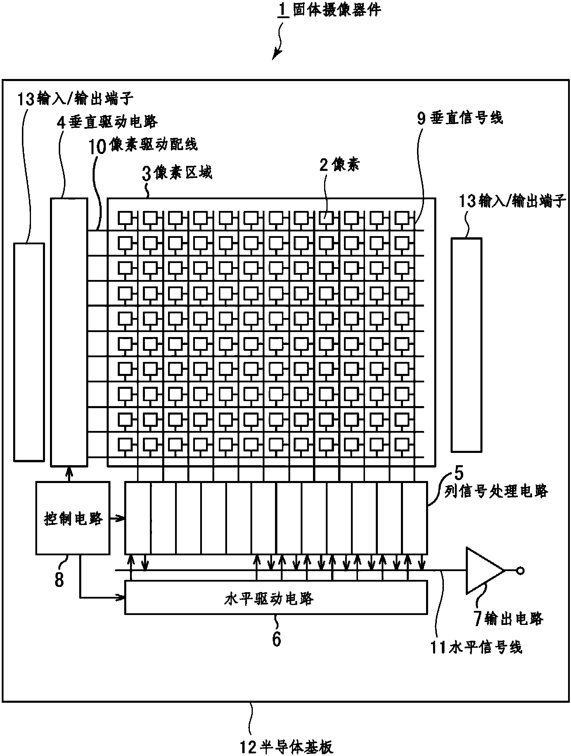
[0021] Schematic configuration example of a solid-state imaging device

[0022] Hereinafter, preferred embodiments of the present invention will be described in detail with reference to the accompanying drawings. Note that, in the specification and the appended drawings, constituent elements that have substantially the same function and structure are denoted with the same reference numerals, and repeated explanation of these constituent elements is omitted.

[0023] figure 1 A schematic configuration of a solid-state imaging device to which an embodiment of the present invention is applied is shown. figure 1 The solid-state imaging device 1 in FIG. 1 is a back-illuminated MOS solid-state imaging device.

[0024] figure 1 The solid-state imaging device 1 includes a semiconductor substrate 12 using silicon (Si) as a semiconductor, a pixel region 3 having pixels 2 arranged in a two-dimensional array on the semiconductor substrate 12 , and peripheral circuit sections around the...


PUM


Abstract

The invention relates to a solid-state imaging device, a method for controlling the same, and an electronic apparatus comprising the same. The solid-state imaging device includes a plurality of pixels which are arranged in a two-dimensional array form and in each of which color separation is performed in a substrate depth direction. The solid-state imaging device includes a pixel addition section which performs addition, when pixel signals of the plurality of pixels are added up to be outputted, by setting addition regions of pixel signals of a first color component to be shifted from addition regions of pixel signals of a second color component at regular intervals. According to the invention, output resolution in the solid-state imaging device performing the color separation in the substrate depth direction can be enhanced.

Description

technical field [0001] The present invention relates to a solid-state imaging device, a control method of the solid-state imaging device, and an electronic device, and in particular, to a solid-state imaging device capable of improving the output resolution of a solid-state imaging device that performs color separation in a substrate depth direction, and a solid-state imaging device control methods and electronic devices. Background technique [0002] There is a solid-state imaging device in which color filters of respective colors are arranged in respective pixels in a Bayer array or the like, and a plurality of colors (usually R, G, and B) are transferred from pixels adjacent to each other as a whole. read out. In recent years, there has also been proposed a solid-state imaging device including pixels each having photoelectric conversion portions for respective plural colors arranged in a substrate depth direction. Thus, this solid-state imaging device is capable of read...

Claims


Application Information

Patent Timeline
15 Jan 2014
Publication
CN103517045A
IPC
H04N9/04; H04N5/374; H04N5/378; H01L27/146; H04N25/46; H04N23/12
CPC
H01L27/14609; H01L27/14647; H04N25/778; H04N23/12; H01L27/14605
Inventors
市川达也; 若林准人