System and method for executing scan test

一种扫描测试、扫描链的技术,应用在扫描测试和存储器内置自测试领域,能够解决产率损失等问题

Active Publication Date: 2014-02-12
NXP USA INC
View PDF8 Cites 20 Cited by
  • Summary
  • Abstract
  • Description
  • Claims
  • Application Information

AI Technical Summary

Problems solved by technology

However, IC10 may still be usable for other package types where the covered block is not necessary for kinetic operation
Therefore, full-scan testing and full-memory BIST testing can lead to unintentional yield loss

Method used


Image

  • System and method for executing scan test
  • System and method for executing scan test
  • System and method for executing scan test

Examples


Embodiment Construction

[0016] The detailed description of the drawings is intended as a description of presently preferred embodiments of the invention and is not intended to represent the only forms in which the invention may be embodied. It is to be understood that the same or equivalent functionality may be achieved by different embodiments, which are intended to be encompassed within the spirit and scope of the invention.

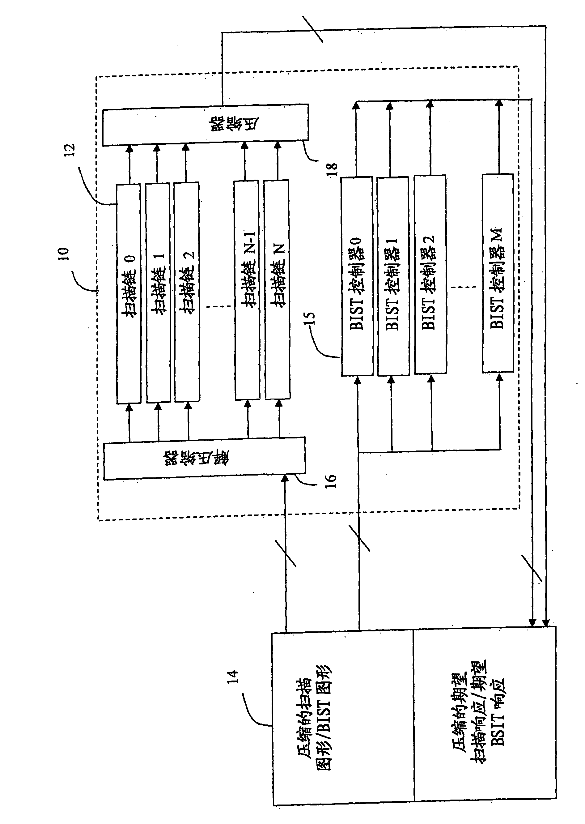
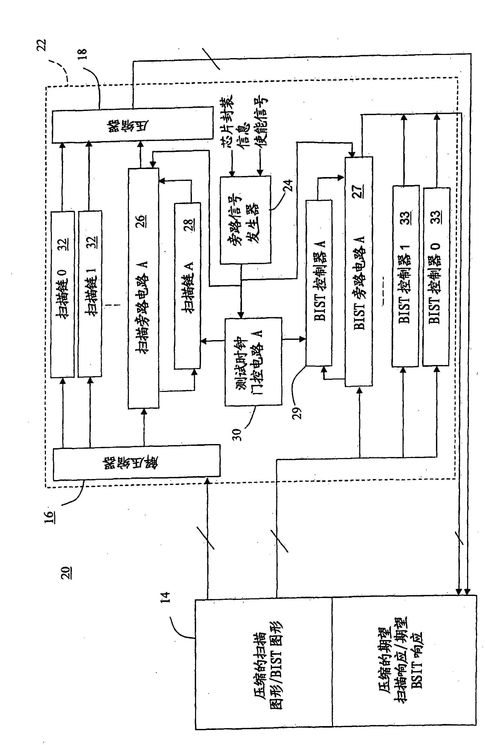
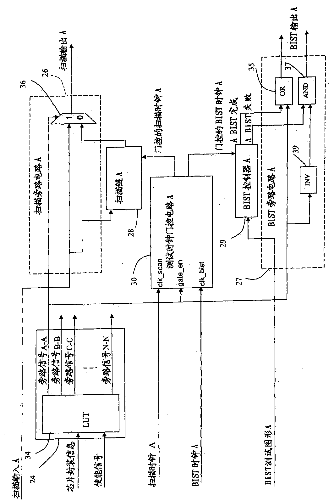
[0017] In one embodiment, the present invention provides a system for performing a scan test, the system including a bypass signal generator and a first scan bypass circuit. The bypass signal generator generates a first bypass signal based on chip package information. The first bypass signal indicates whether a first scan chain associated with a first non-generic IP block of the chip is to be bypassed during scan testing. The first scan bypass circuit bypasses the first scan chain in response to a first bypass signal.

[0018] In another embodiment, the present invention pr...


PUM


Abstract

A system for performing a scan test on an integrated circuit such as a System on a Chip (SoC) that may be packaged in different package types and with different features enabled includes a bypass-signal generator and a first scan-bypass circuit. The bypass-signal generator generates a first bypass signal based on chip package information. The first bypass signal indicates whether a first scan chain associated with a first non-common circuit block of the SoC is to be bypassed. The first scan chain is bypassed in response to the first bypass signal. By enabling partial scan testing based on package information, unintentional yield loss caused by a full scan test determining an SoC is faulty can be avoided.

Description

technical field [0001] The present invention relates generally to scan testing and memory built-in self-test (BIST) of integrated circuits and, more particularly, to systems and methods for performing scan testing and memory BIST testing on integrated circuits using scan bypass and BIST bypass. Background technique [0002] In recent years, there has been tremendous development in the fields of semiconductor devices and electronic circuit integration. Recently, a single system-on-chip (SoC) with multiple packaging types or packaging options is available. In small package embodiments, certain functional intellectual property (IP) blocks may be masked out, depending on the package type selected. These masked IP blocks may include combinational logic blocks and memory blocks. [0003] FIG. 1 illustrates a schematic diagram of a scan test using a scan chain design and a memory test using a BIST controller in a system including a scan test system and a BIST test system. That i...

Claims


Application Information

Patent Timeline
Patent Type & Authority Applications(China)
IPC IPC(8): G01R31/28G11C29/12
CPCG01R31/318536G11C29/32G11C29/40G01R31/318558G01R31/3187
Inventor 万国平章沙雁张旺根
Owner NXP USA INC
Why Eureka
Try Eureka