Imprinted memory
A technology of memory and imprinting method, which is applied in the fields of instruments, semiconductor/solid-state device manufacturing, optics, etc., and can solve the problems that limit the wide application of mask-ROM
- Summary
- Abstract
- Description
- Claims
- Application Information
AI Technical Summary
Problems solved by technology
Method used
Image

Examples
Embodiment Construction
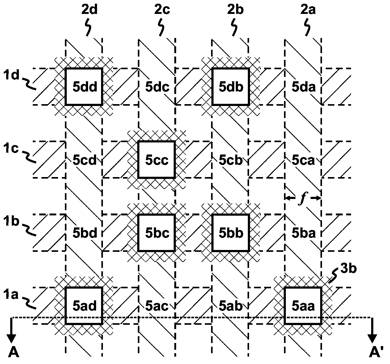
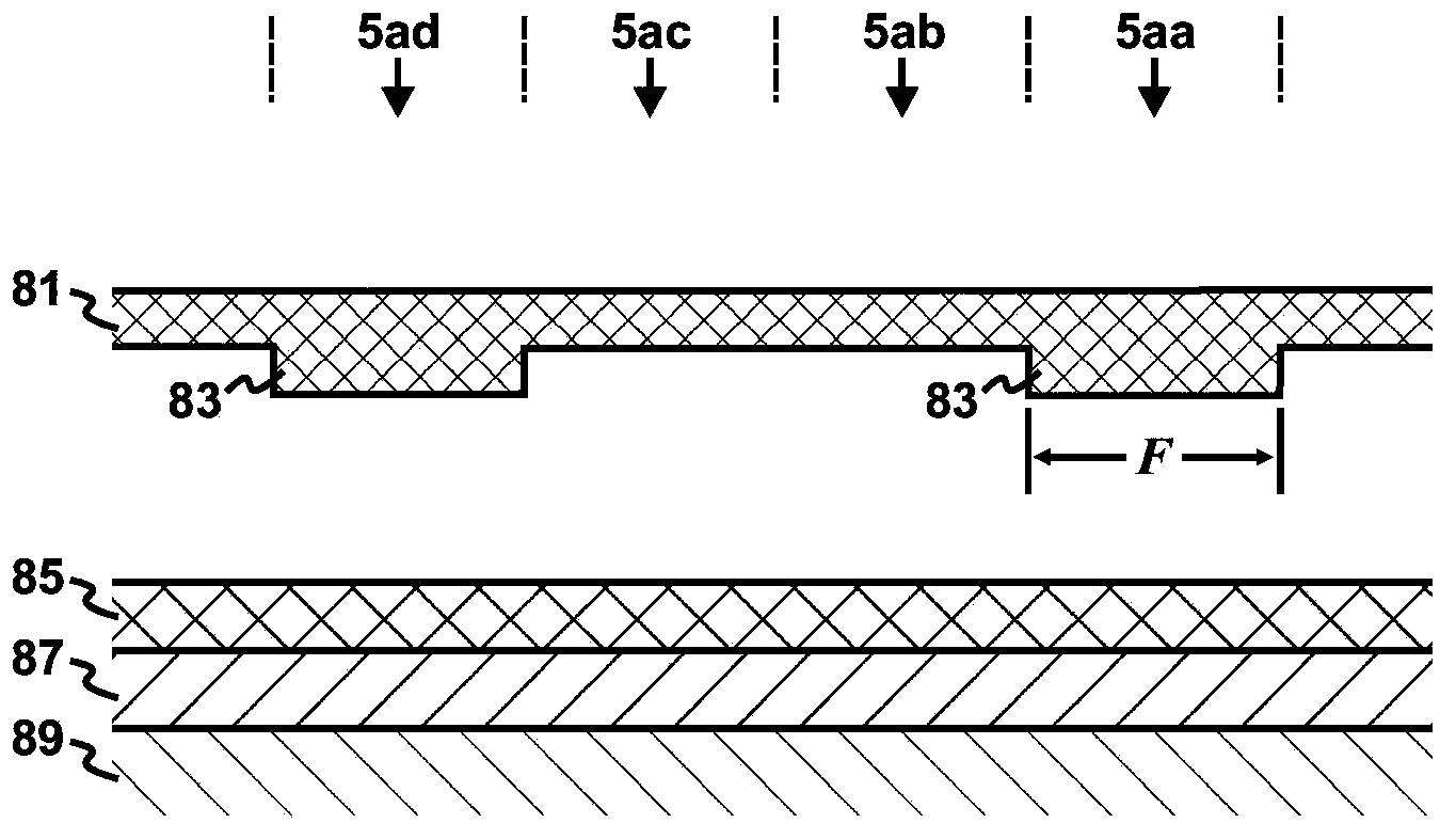
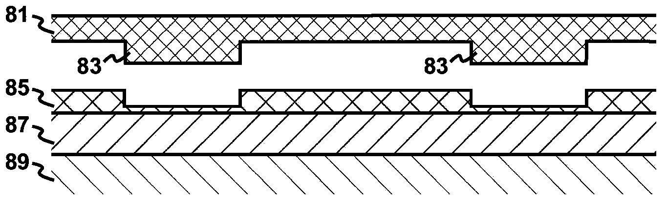
[0015] In order to reduce data entry costs, the present invention proposes an imprinted memory, especially a three-dimensional imprinted memory (3D-iP for short). As far as its final physical structure is concerned, embossed memory is exactly the same as mask-ROM, and they both use data patterns in their data entry film to store data. The difference between imprinted memory and mask-ROM is that they use different data entry methods: mask-ROM uses photolithography, and imprinted memory uses embossing. However, the data templates used in imprinting are much cheaper than the data masks used in photolithography.
[0016] The imprint method achieves graphic conversion by applying pressure on the template to mechanically deform the imprint resist (see Chou et al. "Imprint-lithography with 25-nanometer resolution", Science Magazine, Vol. 272, 5258, pp. 85-87). Examples of imprint methods include thermoplastic nano-imprint lithography, photo nano-imprint lithography, electro-chemica...
PUM
| Property | Measurement | Unit |
|---|---|---|
| Size | aaaaa | aaaaa |
Abstract
Description
Claims
Application Information
 - R&D Engineer
- R&D Manager
- IP Professional
- Industry Leading Data Capabilities
- Powerful AI technology
- Patent DNA Extraction
Browse by: Latest US Patents, China's latest patents, Technical Efficacy Thesaurus, Application Domain, Technology Topic.
© 2024 PatSnap. All rights reserved.Legal|Privacy policy|Modern Slavery Act Transparency Statement|Sitemap