Switchover thin-film transistor with repair function

A technology of thin film transistors and functions, applied in the direction of transistors, circuits, electrical components, etc., can solve problems such as poor performance, false bright lines, etc., achieve the effect of exquisite conception, convenient manufacture, and avoiding adverse phenomena

Inactive Publication Date: 2014-03-26
NANJING CEC PANDA LCD TECH
View PDF3 Cites 6 Cited by
  • Summary
  • Abstract
  • Description
  • Claims
  • Application Information

AI Technical Summary

Problems solved by technology

Currently commonly used switching thin film transistors (Switch TFT) such as figure 1 As shown, the source 2 and the drain 3 are both located on the gate 1, one end of the source 2 is inserted into the open end of the drain 3, the other end of the source 2 is connected to the signal line, and the closed end of the drain 3 is It is also connected to the signal line; in order to increase the driving capability of the switching thin film transistor, the area of ​​the gate 1 is usually enlarged, and the source 2 and the drain 3 are designed to be long and flat. The switching thin film transistor (Switch TFT) has a high probability of poor performance due to its large area. For example, a short circuit between the source 2 and the drain 3 will cause false bright lines.

Method used


Image

  • Switchover thin-film transistor with repair function
  • Switchover thin-film transistor with repair function
  • Switchover thin-film transistor with repair function

Examples


Embodiment Construction

[0018] The present invention will be further described below in conjunction with the accompanying drawings and embodiments.

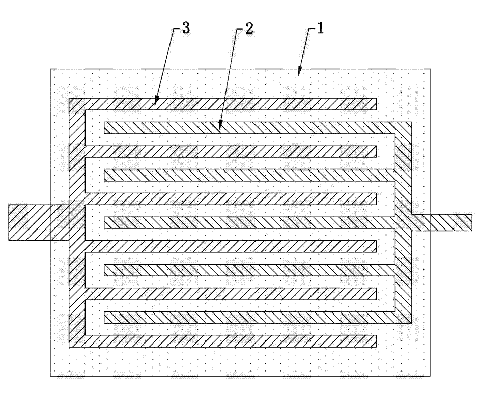
[0019] like image 3 Shown: A switching thin film transistor with repair function, including gate 1, source 2 and drain 3, part of source 2 and part of drain 3 are located on gate 1 and the source on gate 1 2 and the drain 3 on the gate 1 correspond to each other, one end of the source 2 is connected to the signal line and this part of the source 2 is located outside the gate 1, one end of the drain 3 is connected to the signal line and this part of the drain 3 Located outside the gate 1; and the source 2 located outside the gate 1 and the drain 3 located outside the gate 1 correspond to each other. In this structure, the part where the source 2 and the drain 3 are respectively connected to the signal line is arranged outside the gate 1, so that once a short circuit occurs between the source 2 and the drain 3, or between the source 2 or the drain 3 and...


PUM


Abstract

The invention discloses a switchover thin-film transistor with the repair function. The switchover thin-film transistor comprises gate electrodes (1), source electrodes (2) and drain electrodes (3). The switchover thin-film transistor is characterized in that parts of the source electrodes (2) and parts of the drain electrodes (3) are located on the gate electrodes (1), and the source electrodes (2) on the gate electrodes (1) correspond to the drain electrodes (3) on the gate electrodes (1), one end of each source electrode (2) is connected with a signal line and that part of the source electrode (2) is located outside the gate electrode (1), and one end of each drain electrode (3) is connected with a signal line and that part of the drain electrode (3) is located outside the gate electrode (1). In the, switchover thin-film transistor, parts of the source electrodes and the drain electrodes, which are connected with the signal lines, are located outside the gate electrodes, and therefore, the repair can be conducted conveniently. In addition, a plurality of staggered source electrodes and drain electrodes are located on the paired gate electrodes, so the decrease in driving capability caused by repair and the undesirable phenomenon caused by the connection of the drain electrodes to odd and even signal lines are solved. The switchover thin-film transistor has the advantages of skillful design and convenience in manufacturing, and is suitable for promotion and use.

Description

technical field [0001] The invention relates to the technical field of thin film transistors, in particular to a switching thin film transistor with a repairing function which can reduce defective rate and prevent the drive ability from dropping after repair. Background technique [0002] In the field of liquid crystal display manufacturing, switching thin film transistors (Switch TFTs) are usually used as switching elements when driving panels. Panels with switching thin film transistors (Switch TFTs) can save troubles such as terminal cutting or laser cutting. manufacturing steps. Currently commonly used switching thin film transistors (Switch TFT) such as figure 1 As shown, the source 2 and the drain 3 are both located on the gate 1, one end of the source 2 is inserted into the open end of the drain 3, the other end of the source 2 is connected to the signal line, and the closed end of the drain 3 is It is also connected to the signal line; in order to increase the dri...

Claims


Application Information

Patent Timeline
Patent Type & Authority Applications(China)
IPC IPC(8): H01L29/786H01L29/417
CPCH01L29/786H01L29/41733
Inventor 刘文雄
Owner NANJING CEC PANDA LCD TECH
Why Eureka
Try Eureka