A UWB Low Noise Monolithic Integrated Amplifier

A single-chip integrated, low-noise technology, applied in the direction of improving the amplifier to expand the bandwidth, improving the amplifier to reduce the impact of noise, etc., can solve the problems of reducing the service life of the battery, the working bandwidth cannot be satisfied, and the gain is reduced, so as to prolong the service life, Good broadband input and output matching, reducing the effect of parasitic inductance

Active Publication Date: 2017-01-18
SHANGHAI LASERON MICRO ELECTRONICS
View PDF6 Cites 0 Cited by
  • Summary
  • Abstract
  • Description
  • Claims
  • Application Information

AI Technical Summary

Problems solved by technology

However, as the frequency increases and the inductance impedance increases, because the structure uses a bonding wire inductance, the gain is greatly reduced at high frequencies, and the working bandwidth cannot meet the requirements of UWB applications, and the amplifier also works during the data blank period. The service life of the battery is greatly reduced, and the application in the field of mobile communication is also greatly restricted

Method used


Image

  • A UWB Low Noise Monolithic Integrated Amplifier

Examples


Embodiment Construction

[0022] The present invention will be further described below in conjunction with accompanying drawing.

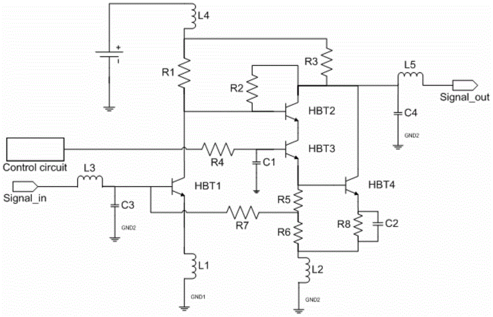
[0023] see figure 1 , an ultra-broadband low-noise monolithic integrated amplifier of the present invention includes a first-stage amplifying circuit and a second-stage amplifying circuit, the first-stage amplifying circuit includes a first transistor HBT1, and the second-stage amplifying circuit includes a second transistor HBT2 and the third transistor HBT3, the present invention also includes a third-stage amplifying circuit, the third-stage amplifying circuit includes a control current input terminal Control circuit, a fourth resistor R4, a first filter capacitor C1 and a fourth transistor HBT4.

[0024] The base of the first transistor HBT1 is connected to the signal input terminal, and the collector of the first transistor HBT1 is the signal output terminal of the first-stage amplifying circuit.

[0025] The collector of the first transistor HBT1 is connected with th...


PUM


Abstract

The invention discloses an ultra-wide-band low-noise singlechip integrated amplifier. The ultra-wide-band low-noise singlechip integrated amplifier comprises a primary amplifying circuit, a secondary amplifying circuit and a tertiary amplifying circuit, wherein the primary amplifying circuit comprises a first triode transistor; the secondary amplifying circuit comprises a second triode transistor and a third triode transistor; the tertiary amplifying circuit comprises a control current inputting end, a fourth resistor, a first filtering capacitor and a fourth triode transistor; the control current inputting end is connected to a base electrode of the third triode transistor through the fourth resistor; the fourth resistor and the base electrode of the third triode transistor are simultaneously grounded through the first filtering capacitor; an emitting electrode of the third triode transistor is connected to a base electrode of the fourth triode transistor; and a collector electrode of the fourth triode transistor is a signal outputting end of the tertiary amplifying circuit. By using the ultra-wide-band low-noise singlechip integrated amplifier, the service life of a battery is greatly prolonged, the parasitic inductance is greatly reduced, high-frequency gain is increased, and a bandwidth range is broadened.

Description

technical field [0001] The invention relates to an integrated amplifier, in particular to an ultra-wideband low-noise monolithic integrated amplifier. Background technique [0002] In the face of tight wireless communication resources, since the FCC (Federal Communications Commission of the United States) allocated the 3.1GHz-10.6GHz frequency band to ultra-wideband UWB (Ultra-Wide Band) and approved ultra-wideband UWB civilian use, wireless personal area network (WPAN) ), home network connection and short-range radar and other fields have achieved rapid development, and thus have broad market application prospects. [0003] At present, there are two main methods of ultra-wideband communication. One is pulse ultra-wideband, which uses short-time impact pulses as information carriers, and carries information through PPM, PAM, etc. Modulation at the nanosecond level) to obtain very wide bandwidth; the other is multi-band ultra-wideband, which carries information through MB-OF...

Claims


Application Information

Patent Timeline
Patent Type & Authority Patents(China)
IPC IPC(8): H03F1/42H03F1/26
Inventor 刘金刚
Owner SHANGHAI LASERON MICRO ELECTRONICS
Why Eureka
Try Eureka