Imaging element module and method for manufacturing same

A technology of an imaging element and a manufacturing method, which is applied in the directions of electrical components, assembling printed circuits with electrical components, and image communication, etc., can solve the problems of contamination of the light-receiving surface, difficulty in storage, and no consideration.

Inactive Publication Date: 2014-04-30
FUJIFILM CORP
View PDF11 Cites 9 Cited by
  • Summary
  • Abstract
  • Description
  • Claims
  • Application Information

AI Technical Summary

Problems solved by technology

However, by covering with resin, the thickness of the imaging device module is further increased by the amount corresponding to the resin, and it is difficult to house it in a narrow case.
Therefore, it is necessary to consider what thickness of resin to cover, but this patent document 1 does not consider this.
[0009] In addition, as described in FIG. 6 of Patent Document 1, when the back side of the imaging element chip is covered with resin, when the resin is filled, the resin may leak from between the peripheral portion of the opening of the wiring board and the peripheral portion of the imaging element chip. The formed gap flows into the light-receiving surface side and contaminates the light-receiving surface, but this is not considered in Patent Document 1
If the image sensor chip is large, even if the resin protrudes to the periphery of the light-receiving surface, it will not be a problem. However, the smaller the image sensor chip is, the more it will become a problem.

Method used


Image

  • Imaging element module and method for manufacturing same
  • Imaging element module and method for manufacturing same
  • Imaging element module and method for manufacturing same

Examples


Embodiment Construction

[0024] Hereinafter, one embodiment of the present invention will be described with reference to the drawings.

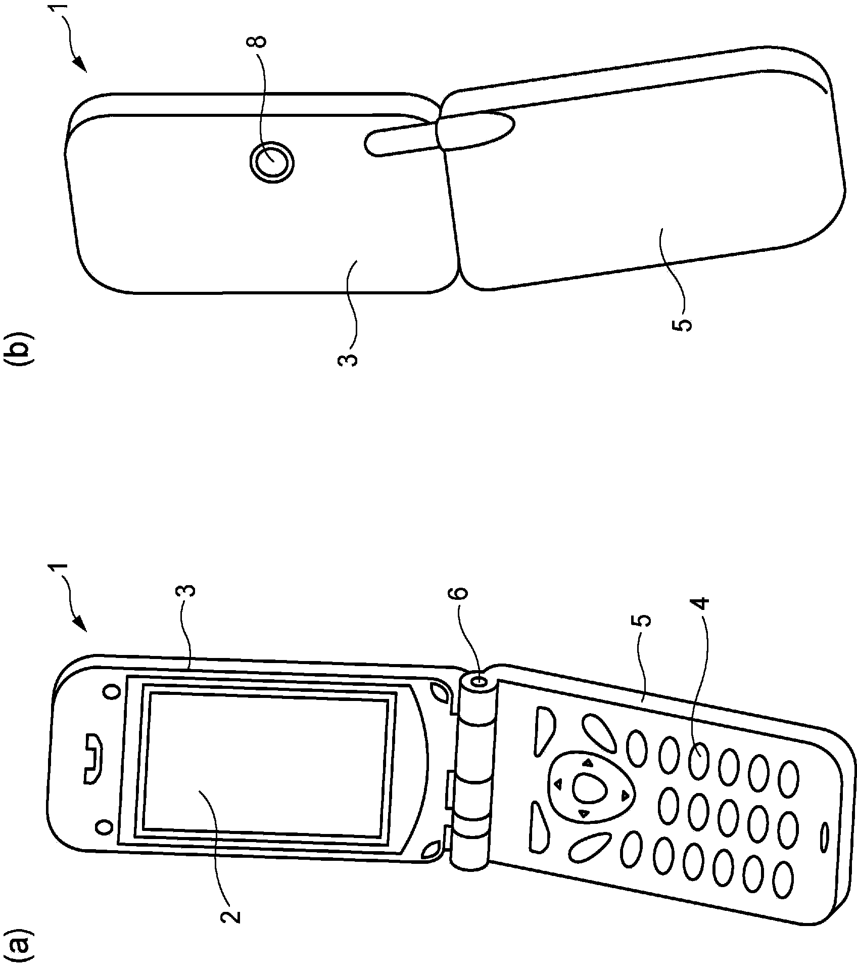
[0025] figure 1 (a) and (b) are external views of a foldable mobile phone, which is an example of a small electronic device equipped with an imaging device module according to an embodiment of the present invention. In this foldable mobile phone 1 , an upper housing 3 on which a liquid crystal display unit 2 is mounted and a lower housing 5 on which keys 4 and the like are mounted are foldably connected by a hinge portion 6 .

[0026] The liquid crystal display unit 2 of the upper housing 3 is constituted by a large display device covering most of the front side of the upper housing 3 , and a camera (imaging element) module is also incorporated in the upper housing 3 . figure 1 (b) shows the back side of the mobile phone 1 , and the photographing lens 8 of the camera is exposed from the opening on the back side of the upper housing 3 . That is, since the camera m...


PUM

PropertyMeasurementUnit
particle diameteraaaaaaaaaa

Abstract

The front face of an opening (12) in a first wiring board (11) is covered by a transparent substrate (15), a light-receiving face is made to face the opening (12) of the first wiring board (11), and an imaging element chip (13) is flip-chip bonded to the rear face side of the first wiring board (11). A gap (18) formed between connection terminals (14) between the periphery of the light-receiving face of the imaging element chip (13) and the peripheral edge section of the opening (12) in the first wiring substrate (11) is buried in a first resin, and the entire rear face of the imaging element chip (13) and the rear face side of the first wiring substrate (11) are covered by a second resin (30) (30a). At the front face on this rear face side, an exposed conductive portion substantially parallel with the front face of the transparent substrate (15) is covered with the second resin (30). A second wiring substrate (22) is electrically and mechanically connected to the first wiring substrate (11).

Description

technical field [0001] The present invention relates to an imaging element module mounted on electronic equipment such as a mobile phone with a camera and a method of manufacturing the same. Background technique [0002] As described in Patent Documents 1 and 2, when an imaging device module is mounted on an electronic device, a photographic lens unit is provided on the front of the light receiving surface of the imaging device module. The lens-equipped imaging device module is attached to the inner surface of the housing on the back side of the electronic device, and the front end of the camera unit is attached so as to be flush with the housing surface. That is, conventionally, it is possible to use the entire thickness of the housing of the electronic device from the front side to the back side for the camera. [0003] However, in recent years, multi-functionalization and thinning have been progressing, such as cellular phones with cameras, and the space for mounting ima...

Claims


Application Information

Patent Timeline
Patent Type & Authority Applications(China)
IPC IPC(8): H04N5/225H04N5/369
CPCH05K3/30H01L27/14618H04N5/2257H04N5/2253H01L2924/0002Y10T29/4913H04N23/57H04N23/54H01L2924/00
Inventor 滨田秀岛村均高濑善幸
Owner FUJIFILM CORP
Why Eureka
Try Eureka