Spatial light modulator and light field three-dimensional display system thereof
A technology of spatial light modulator and light, which is applied in optics, instruments, optical components, etc., can solve the problems of complex liquid crystal process and difficulty in mass production, and achieve high resolution, large reproduction depth, and high deflection accuracy Effect
- Summary
- Abstract
- Description
- Claims
- Application Information
AI Technical Summary
Problems solved by technology
Method used
Image
Examples
Embodiment 1
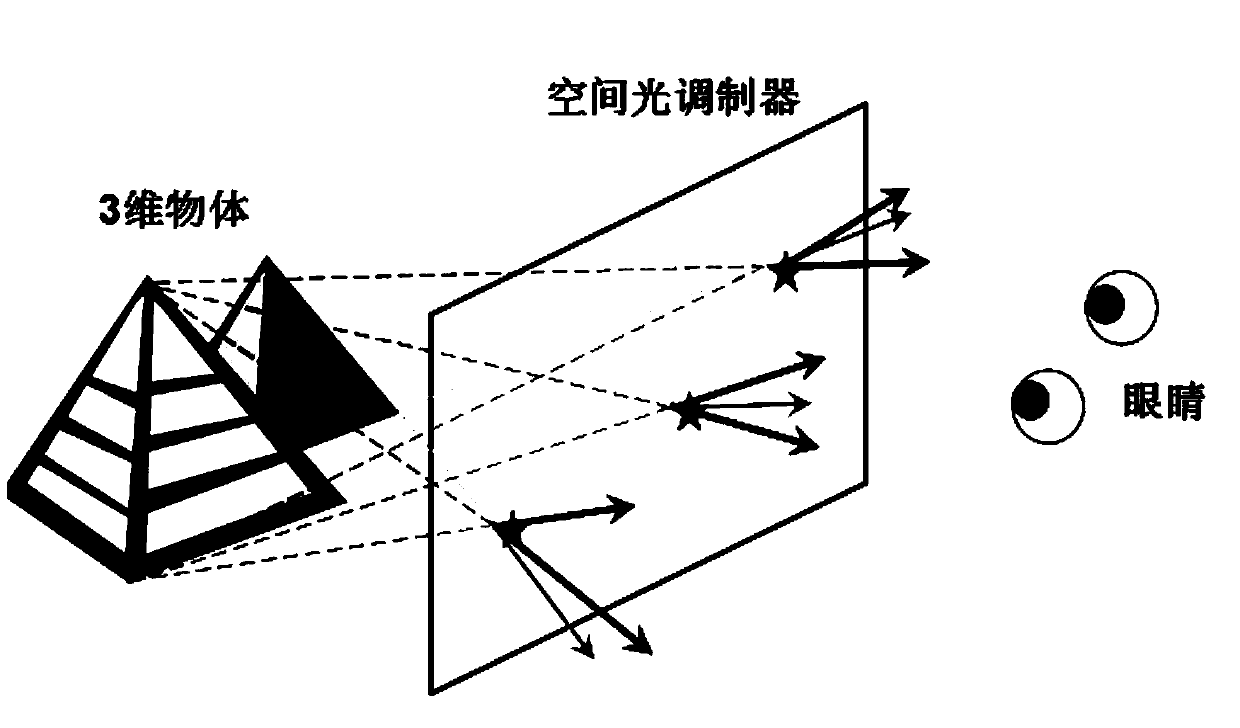
[0050] Such as figure 1 Shown is the principle diagram of the light field display in this embodiment; in this embodiment: the spatial light modulator 11 simulates the light emitted by the three-dimensional object 10 through each pixel unit 12 to reproduce a three-dimensional image.
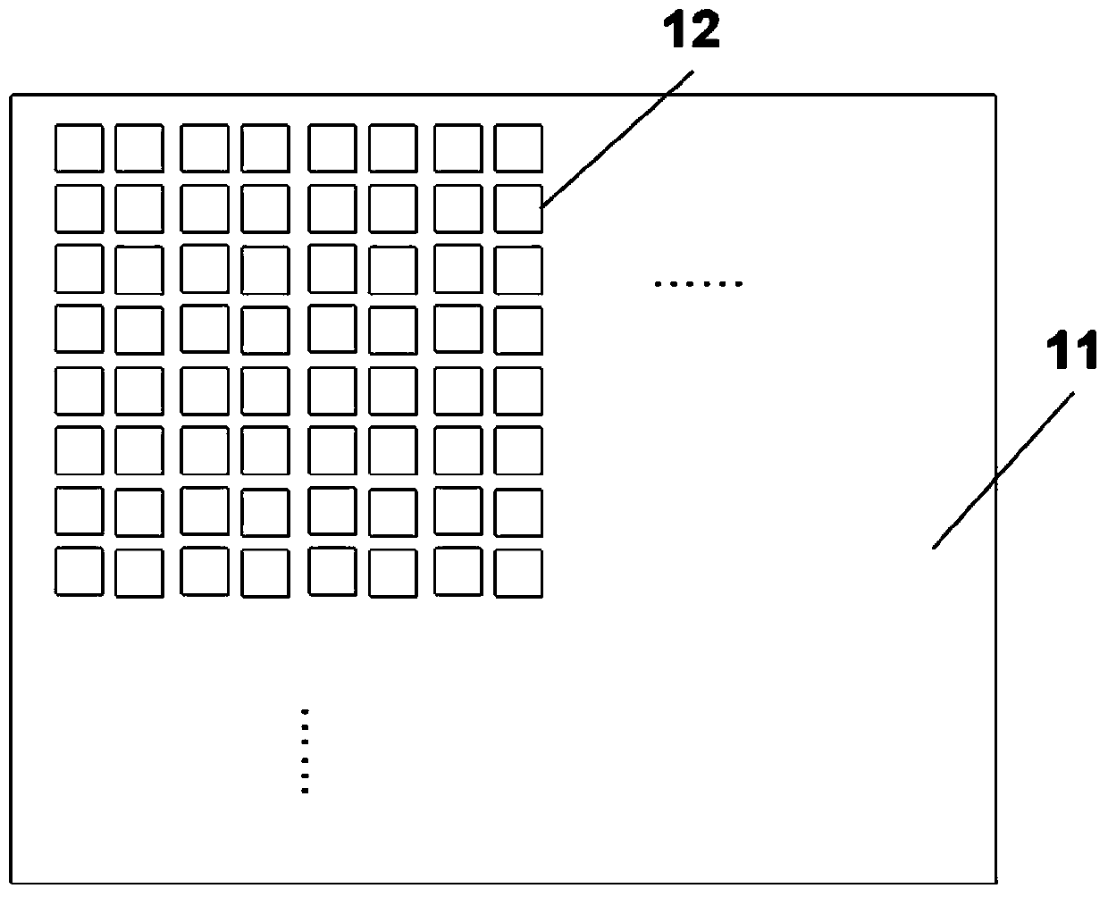
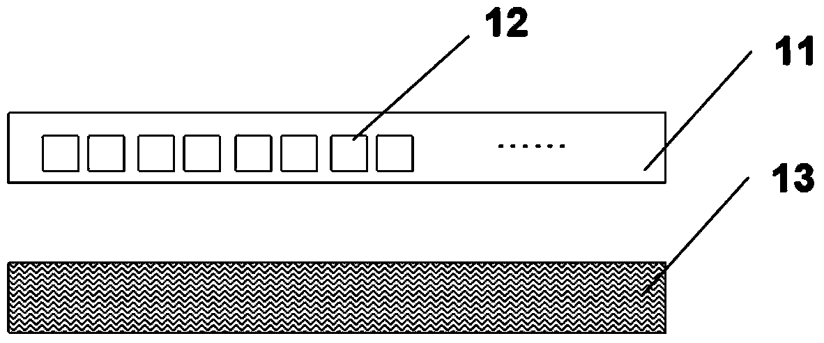
[0051] Such as figure 2 with image 3 As shown, the spatial light modulator 11 is a two-dimensional array composed of pixel units 12 . image 3 It is another overall structure diagram of the spatial light modulator, wherein: the spatial light modulator 11 is a one-dimensional array composed of pixel units 12, which is expanded into a simulated two-dimensional array in cooperation with the mechanical scanning device 13.
[0052] Such as Figure 4 As shown, each pixel 12 of the spatial light modulator is an intensity modulator 14 and a light deflector 15 . When the light emitted by the light source 13 passes through the spatial light modulator, its intensity and direction are modulated by 14 an...
Embodiment 2
[0064] Figure 10 is the structure of the blue-phase liquid crystal light deflector in the second example figure 1 . The blue phase liquid crystal 20 is sandwiched between the upper substrate 16 and the lower substrate 17 . Inside the upper substrate 16 are triangular first electrodes 18 and triangular third electrodes 23 , and inside the lower substrate 17 are triangular second electrodes 19 and triangular fourth electrodes 24 . The triangular first electrode 18 is complementary in shape to the triangular third electrode 23, but separated by a distance of 10 microns to 5 mm. The triangular second electrode 19 is complementary in shape to the triangular fourth electrode 24, but separated by a distance of 10 microns to 5 mm. The light propagates along the z direction, parallel to the upper substrate 16 and the lower substrate 17 . The first electrode 18 and the second electrode 19 are aligned, and the angle between their hypotenuse and the light propagation direction is θ ...
PUM
| Property | Measurement | Unit |
|---|---|---|
| Thickness | aaaaa | aaaaa |
| Thickness | aaaaa | aaaaa |
Abstract
Description
Claims
Application Information


