

A kind of composite structure and manufacturing method based on ce:yag chip
一种复合结构、制作方法的技术,应用在光学领域,能够解决效用降低、波长单一等问题,达到成本低、时间特性好、显色效果好的效果
- Summary
- Abstract
- Description
- Claims
- Application Information
AI Technical Summary
Problems solved by technology
Method used
Image

Examples
Embodiment 1
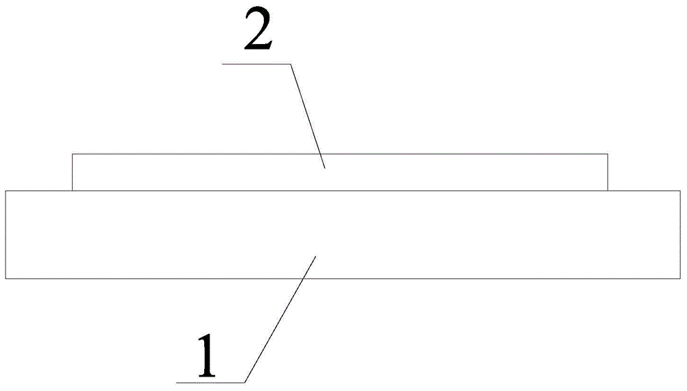
[0031] Eu:Y Plating by Sputtering 2 o 3 film, first prepare powdered Eu:Y 2 o 3 , wherein the molar concentration of Eu ions is 0.2%, and it is prepared into a bulk target by pressing method, and Eu:Y 2 o 3 The target is fixed on the cathode of the coating machine, and the Ce:YAG wafer (wherein the molar concentration of Ce ions is 0.3%) is cut and polished into the required size by the pulling method, and the cleaned Ce:YAG wafer is Fix it on the anode facing the target surface, then pump the system to high vacuum (10 -3 Pa) and then filled with argon gas of 5 Pa, apply a voltage between the cathode and the anode, start the coating, vacuumize after the coating is completed, then fill in nitrogen for cold cutting, and finally get the Eu:Y coating 2 o 3 Ce:YAG wafer composite light-emitting structure of red light-emitting film.
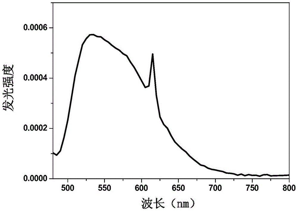
[0032] figure 2 Plating Eu:Y for Example 1 2 o 3 The emission spectrum of the film composite structure, as can be seen from the figure, the...
Embodiment 2
[0034] Glue-coating method to plate red phosphor film, add 0.05% by weight red phosphor to the silica gel, stir evenly, and evenly cover the Ce:YAG wafer by spraying (wherein the molar concentration of Ce ions is 0.3%, The surface of the Ce:YAG wafer is prepared by a temperature gradient method, and then baked at 120° C. for 3 hours. After the glue is cured, a Ce:YAG wafer composite light-emitting structure coated with a red phosphor film is obtained.
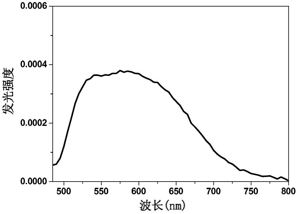
[0035] image 3 It is the emission spectrum diagram of the combination structure of the red-light phosphor coating film in the glue-coating mode of embodiment 2. It can be seen from the figure that the combined structure of the glue-coating red phosphor powder film coating has an emission spectrum with a width of 500nm to 750nm, and can realize the emission spectrum from green to green. Luminescence in the light to red band.
Embodiment 3
[0037] Bond the Eu:YAG wafer (where the molar concentration of Eu ions is 0.2%, prepared by the Kyroplasty method) and the Ce:YAG wafer (where the molar concentration of Ce ions is 0.5%, which is prepared by the temperature gradient method) with silica gel. Surface polishing of Ce:YAG wafer and Eu:YAG wafer to make it have good smoothness and flatness, coating the surface of Ce:YAG wafer with silica gel, covering with Eu:YAG wafer, and baking at 100°C for 3 hours, Then slowly cool down to room temperature to form a Ce:YAG and Eu:YAG wafer composite light-emitting structure.
[0038] Figure 4 It is the emission spectrum diagram of the combined structure of silica gel bonded with Eu:YAG wafer in Example 3. It can be seen from the figure that the combined structure of silica gel bonded with Eu:YAG wafer has an emission spectrum with a width of 500nm to 700nm, which can realize the emission spectrum from green light to red light. bands of glow.
PUM
| Property | Measurement | Unit |
|---|---|---|
| width | aaaaa | aaaaa |
| spectroscopy | aaaaa | aaaaa |
| spectroscopy | aaaaa | aaaaa |
Abstract
Description
Claims
Application Information