Printed circuit board pad

A technology of printed circuit boards and pads, which is applied in the direction of printed circuit components, electrical connection printed components, etc., can solve problems such as difficulty in meeting the requirements for mounting electronic components of different specifications, and achieve the effect of saving space resources

Inactive Publication Date: 2014-05-21
PHICOMM (SHANGHAI) CO LTD
View PDF4 Cites 11 Cited by
  • Summary
  • Abstract
  • Description
  • Claims
  • Application Information

AI Technical Summary

Problems solved by technology

[0004] The technical problem to be solved by the present invention is to overcome the defect that the same pad of the traditional printed circuit board in the prior art is difficult to meet the requirements of mounting electronic components of different specifications, and to provide a method that can be mounted on the same pad. Printed circuit board pads of electronic components of different specifications

Method used


Image

  • Printed circuit board pad
  • Printed circuit board pad

Examples


Embodiment Construction

[0020] The preferred embodiments of the present invention are given below in conjunction with the accompanying drawings to describe the technical solution of the present invention in detail.

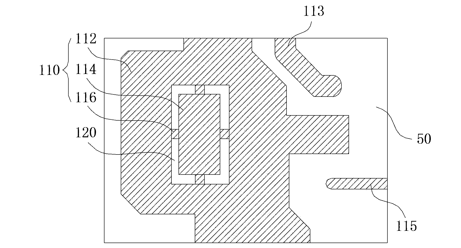
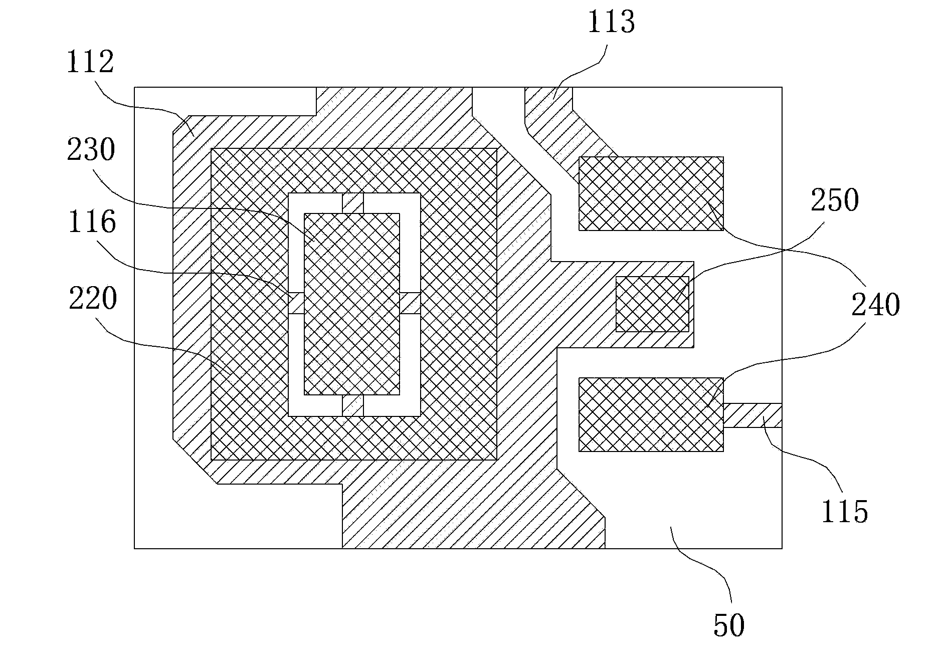
[0021] Such as figure 1 and figure 2 As shown, the pads of the printed circuit board according to the preferred embodiment of the present invention include a large pad and at least one small pad. Usually, the large pads and the small pads are disposed on the printed circuit board 50 . The large pad includes a copper skin layer 110, and the copper skin layer 110 includes an outer ring copper skin 112, an inner ring copper skin 114 surrounded by the outer ring copper skin 112, and a copper wire 116 connecting the inner ring copper skin 114 and the outer ring copper skin 112 . A gap 120 is provided between the inner ring copper skin 114 and the outer ring copper skin 112 . The outer copper skin 112 and the inner copper skin 114 are respectively provided with tin layers to form the firs...


PUM


Abstract

The invention discloses a printed circuit board pad comprising a big pad and at least one small pad; the big pad comprises a copper layer; the copper layer comprises an outer copper layer, an inner copper layer wrapped by the outer copper layer and a copper layer wire connecting the inner copper layer with the outer copper layer; a gap is arranged between the inner copper layer and the outer copper layer; the outer copper layer and the inner copper layer are respectively provided with a tin layer so as to form a first sub pad and a second sub pad; the small pad is arranged one side, extending in a width direction, of the big pad. The printed circuit board pad is provided; the first sub pad is used for pastering electric elements with big sizes; the second sub pad is used for pastering electric elements with small sizes; the printed circuit board pad can paster at least two kinds of electric elements with different specifications, thereby saving space resources of the printed circuit board.

Description

technical field [0001] The invention relates to the field of printed circuit board manufacturing, in particular to a printed circuit board welding pad. Background technique [0002] With the development of electronic technology, printed circuit boards are more and more widely used in the electronic field. Pads are an important part of printed circuit boards and are used to mount electronic components. During the installation process of electronic components, the specifications of electronic components are usually selected according to actual needs, so that the selected electronic components can not only meet the requirements, but also avoid excessive margins, resulting in waste of resources. However, the size of the pad is often fixed during the manufacture of the printed circuit board, and the size of electronic components of different specifications may vary greatly. Since the solder on the pad is liquid at high temperature, when a smaller-sized electronic component is m...

Claims


Application Information

Patent Timeline
Patent Type & Authority Applications(China)
IPC IPC(8): H05K1/11
Inventor 陈铭
Owner PHICOMM (SHANGHAI) CO LTD
Why Eureka
Try Eureka