A detection device for preventing wafer fragmentation

A detection device and chip technology, which is applied to electrical components, semiconductor/solid-state device manufacturing, circuits, etc., can solve problems such as chip and chip storage cavity fragmentation, chip processing process is wasted, etc., and achieve the effect of improving production efficiency

Active Publication Date: 2016-09-28
SHANGHAI HUAHONG GRACE SEMICON MFG CORP
View PDF7 Cites 0 Cited by
  • Summary
  • Abstract
  • Description
  • Claims
  • Application Information

AI Technical Summary

Problems solved by technology

Once there is a deviation in the placement position of the wafer on the carrier table 121, and there is no detection equipment to detect it, when the lifting device 122 drives the wafer carrier table 121 to rise or fall, it will cause the wafer and the wafer to be stored together. The inner walls of the cavity 12 are rubbed and cracked, which means that the previous wafer processing process is all in vain

Method used


Image

  • A detection device for preventing wafer fragmentation
  • A detection device for preventing wafer fragmentation
  • A detection device for preventing wafer fragmentation

Examples


Embodiment Construction

[0023] The following combination image 3 and Figure 4 , taking the P5000 semiconductor device as an example, the specific implementation manner of the present invention will be described in detail.

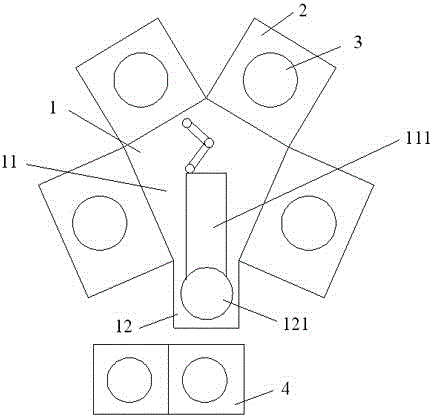
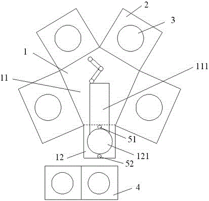
[0024] Such as image 3 As shown, the P5000 semiconductor equipment is a semiconductor equipment with multiple processing chambers, capable of accommodating and processing 5-inch, 6-inch or 8-inch wafers. It includes a transfer chamber 1, and four processing chambers 2 arranged around the transfer chamber 1 in a star shape. Each processing chamber 2 is respectively connected to the transfer chamber 1 through an isolation valve, and each processing chamber 2 is respectively provided with a loading platform 3 for carrying and positioning the wafer when processing the wafer.

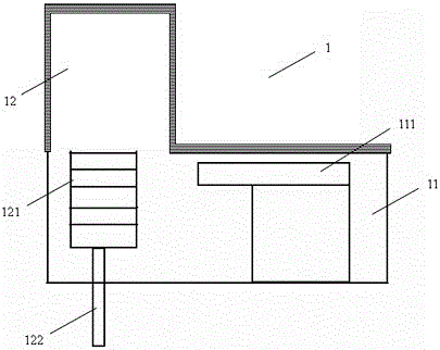
[0025] Such as image 3 and 4 As shown, the transfer chamber 1 includes a wafer transfer buffer chamber 11 and a wafer storage chamber 12 , and the top of the wafer storage chamber 12 is higher than the ...


PUM


Abstract

The invention relates to a detection device used for preventing a wafer from fragmenting. The detection device is used by semiconductor equipment having multiple processing chambers. The semiconductor equipment comprises a transmission chamber and a plurality of processing chambers arranged at periphery of the transmission chamber in a star-shaped mode, the transmission chamber comprises a wafer transmission buffer chamber and a wafer storage chamber, the detection device is arranged in the wafer storage chamber and is used for detecting whether the wafer arranged in the wafer storage chamber has position deviation, and the detection device comprises a first sensor, a first receiver used for receiving a detection signal emitted by the first sensor, a second sensor and a second receiver used for receiving a detection signal emitted by the second sensor. The detection device can effectively detect whether the wafer arranged in the wafer storage chamber has disposing position deviation, so a problem of discard because of fragmentation caused by friction between the wafer and the inner wall of the wafer storage chamber is settled, and production efficiency of the semiconductor equipment can be effectively improved.

Description

technical field [0001] The invention belongs to the technical field of semiconductor manufacturing, and relates to a detection device applied to semiconductor equipment, in particular to a detection device used in semiconductor equipment with multiple processing chambers to prevent wafer fragmentation. Background technique [0002] In the prior art, most of the vacuum semiconductor process equipment suitable for multi-processing chambers are used to perform chemical vapor deposition on the surface of the wafer, such as figure 1 As shown, it includes a transfer chamber 1, and several processing chambers 2 arranged around the transfer chamber 1 in a star shape. Each processing chamber 2 is respectively connected to the transfer chamber 1 through an isolation valve, and each processing chamber 2 is respectively provided with a loading platform 3 for carrying and positioning the wafer when processing the wafer. [0003] At present, the most commonly used single-wafer, multi-cha...

Claims


Application Information

Patent Timeline
Patent Type & Authority Patents(China)
IPC IPC(8): H01L21/67
CPCH01L21/67259
Inventor 马东解毅赵洪涛何雅彬马世余王喆沈瑜俊吴奇昆孙亭
Owner SHANGHAI HUAHONG GRACE SEMICON MFG CORP
Why Eureka
Try Eureka