Practical level switching circuit

A technology for converting circuits and levels, applied in the direction of logic circuit coupling/interface and logic circuit connection/interface layout using field effect transistors, which can solve the problems of complicated application design and increased cost, and achieve simplified circuit design and reduced cost effect

Inactive Publication Date: 2014-06-25
SHENZHEN BOYONG TECH
View PDF3 Cites 8 Cited by
  • Summary
  • Abstract
  • Description
  • Claims
  • Application Information

AI Technical Summary

Problems solved by technology

[0002] Existing integrated circuits have strict requirements on power domains when they are applied in multiple chips and multiple power domains. For chips with inconsistent voltage ranges, if communication is performed, a dedicated chip is required for level conversion, or a resistor is used to implement pull-up / pull-down, this application increases cost and complicates application design

Method used


Image

  • Practical level switching circuit

Examples


Embodiment Construction

[0010] The present invention will be further described below in conjunction with the accompanying drawings.

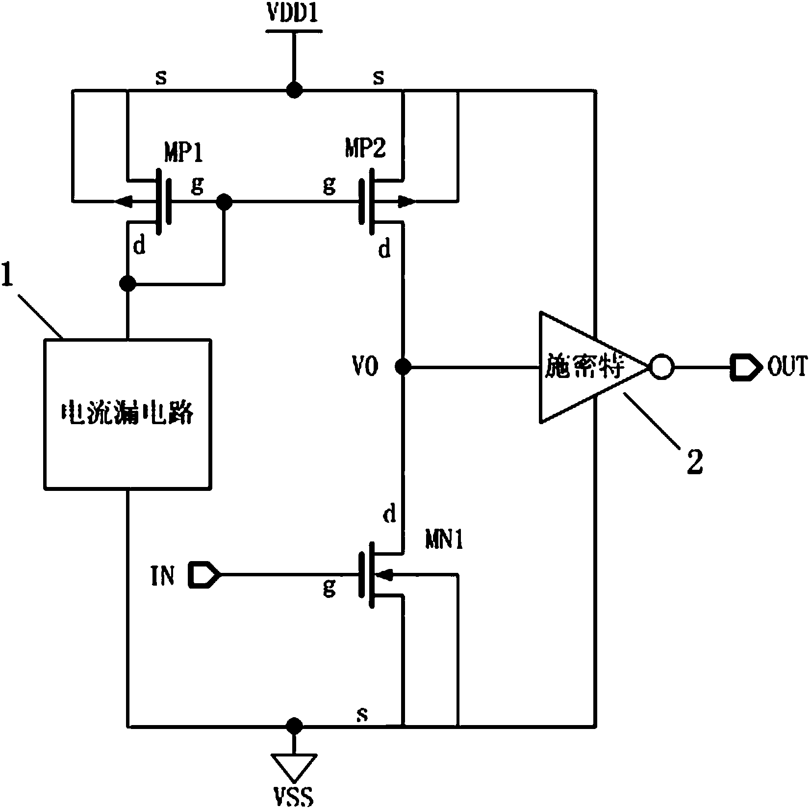
[0011] Please refer to figure 1 , The practical level conversion circuit of the present invention includes a current leakage circuit 1, a Schmitt trigger 2, a PMOS transistor MP1, a PMOS transistor MP2, and an NMOS transistor MN1.

[0012] Wherein, the source of the PMOS transistor MP1, the source of the PMOS transistor MP2, and the high level pin of the Schmitt trigger 2 are all connected to the logic high level VDD1, and the gate of the PMOS transistor MP1, the gate of the PMOS transistor MP2, and the gate of the PMOS transistor MP2 are all connected to the logic high level VDD1. The MP1 drain is connected to the input end of the current leakage circuit 1, the drain of the PMOS transistor MP2 and the NMOS transistor MN1 are connected to the input end of the Schmitt trigger 2, the output end of the current leakage circuit 1, Both the source of the NMOS transistor MN1...


PUM


Abstract

The invention discloses a practical level switching circuit which comprises a current leakage circuit, a Schmitt trigger, a PMOS tube MP1, a PMOS tube PM2 and an NMOS tube MN1. In the practical level switching circuit, the PMOS tube MP1 and the PMOS tube MP2 form a current mirror and enable the electric potential of the input end of the Schmitt trigger to be pulled up to a logic high level VDD1, the NMOS tube MN1 is used for pulling down the electric potential of the input end of the Schmitt trigger to a logic low level VSS, and the Schmitt trigger is used for shaping and inversion and enabling an output signal OUT and an input signal IN to be consistent in phase. Therefore, direct communication between multiple power domain chips is achieved, a special voltage conversion chip or a pull-up/pull-down resistor is not needed, circuit design is simplified, and the cost is lowered.

Description

technical field [0001] The invention relates to the technical field of level conversion circuits, in particular to a practical level conversion circuit. Background technique [0002] Existing integrated circuits have strict requirements on power domains when they are applied in multiple chips and multiple power domains. For chips with inconsistent voltage ranges, if they communicate, a dedicated chip is required for level conversion, or a resistor is used to implement pull-up / Pull-down, this application adds cost and complicates application design. Contents of the invention [0003] The purpose of the present invention is to provide a practical level conversion circuit that can realize direct communication between chips in multiple power domains and does not require a dedicated voltage conversion chip or pull-up / pull-down resistors. [0004] In order to achieve the above object, the present invention provides a practical level conversion circuit, including a current leak...

Claims


Application Information

Patent Timeline
Patent Type & Authority Applications(China)
IPC IPC(8): H03K19/0185
Inventor 刘成军
Owner SHENZHEN BOYONG TECH
Why Eureka
Try Eureka