Chip bonding pad layout design method suitable for multiple different encapsulation requirements

A chip pad and layout design technology, which is applied in the manufacture of electrical components, electrical solid devices, semiconductor/solid devices, etc., can solve the problems of small number of pads, overlapping, and different shapes, so as to provide flexibility and reduce costs Effect

Active Publication Date: 2014-07-02
EAST CHINA INST OF OPTOELECTRONICS INTEGRATEDDEVICE
View PDF6 Cites 3 Cited by
  • Summary
  • Abstract
  • Description
  • Claims
  • Application Information

AI Technical Summary

Problems solved by technology

In the chip layout design, the position of the chip pad is generally arranged according to a selected package type, such as a dual in-line package (DIP) or a surface mount package (SOP), until the layout design is completed Finally, it is necessary to use a selected package type for pressure welding. Once the chip is required to adopt other package forms, because the inner cavity and lead frame of different package types are different, the layout pads cannot meet the needs of different packages. Type requirements, especially the pads at the four corners of the chip, it is easy to overlap with the adjacent pads during pressure welding
Chinese patent CN102237282A "a non-contact IC chip Pad layout design method" adopts the design of two adjacent pads to diagonal positions to meet the requirements of making the chip adapt to different packages, but its application conditions have many restrictions: 1. ) The number of pads is small: 2 pads; 2) The order of the pads: there is no requirement for the sequence of the pads, as long as the position of the pads is the upper and lower diagonal positions, regardless of the left and right; The package cavity is basically the same
Therefore, it is not suitable for multiple chip pads with sequential requirements and widely different package types (not only different shapes, but also different inner cavities), and this method does not produce a better effect

Method used


Image

  • Chip bonding pad layout design method suitable for multiple different encapsulation requirements
  • Chip bonding pad layout design method suitable for multiple different encapsulation requirements
  • Chip bonding pad layout design method suitable for multiple different encapsulation requirements

Examples


Embodiment Construction

[0027] The present invention will be further described below in conjunction with the accompanying drawings. The following examples are only used to illustrate the technical solution of the present invention more clearly, but not to limit the protection scope of the present invention.

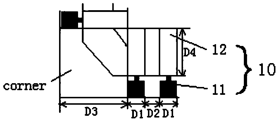
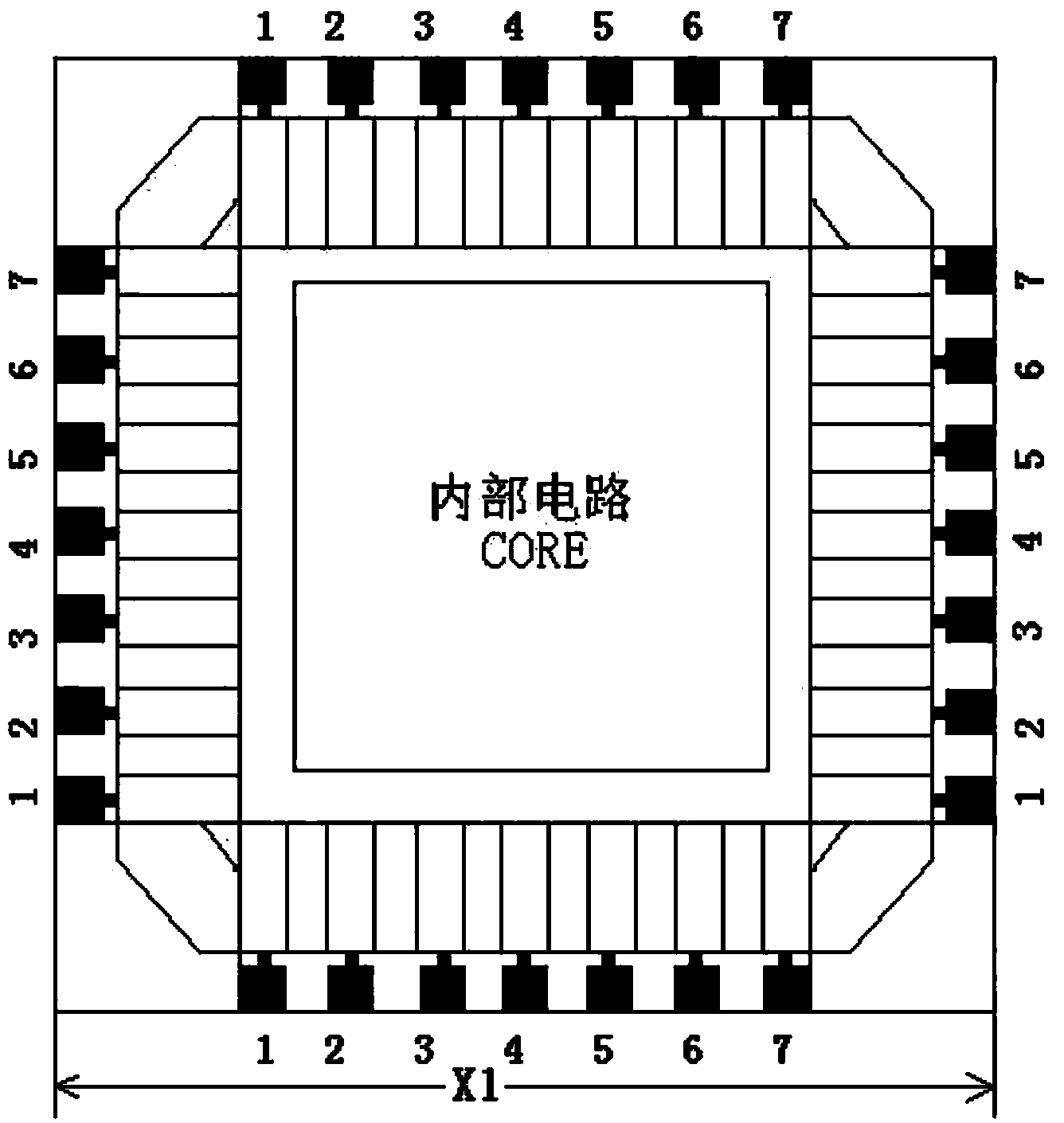
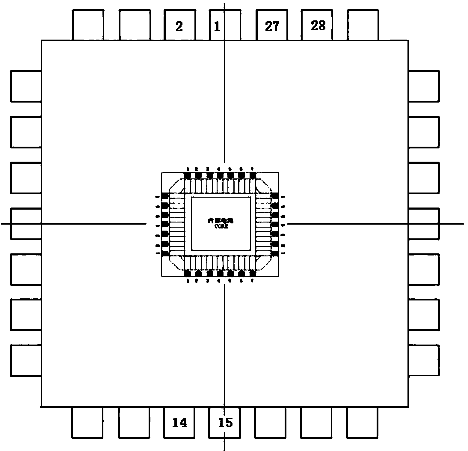
[0028] 1. Determine the total number of pads of the chip and the number of pads on each side: determine the total number of pads (N) of the chip, including necessary (such as input, output), redundant (such as multiple power supplies, grounds), available Selected (such as intermediate test), etc.; according to the total number of pads, roughly determine the number of pads on each side and the size of the chip in the length and width direction.

[0029] 2. Determine the basic package type: According to the total number of pads and the chip area, select a variety of package types that meet the requirements of the lumen size and lumen lead frame, and select a package type as the basic package type....


PUM


Abstract

The invention discloses a chip bonding pad layout design method suitable for multiple different encapsulation requirements. According to the total number of bonding pads, the number of the bonding pads at each side of a chip and the dimensions of the chip in the length direction and in the width direction are determined; a basic encapsulation type is determined; the number and the positions of the bonding pads at each side of the chip are adjusted; another encapsulation type is selected, and a bonding figure is designed; optimizing methods of bonding the different bonding pads that the bonding pads with the bonding problem or different encapsulation types are replaced by moving the bonding pad positions with the bonding problem and increasing the number of the bonding pads are adopted, so that the bonding pads can meet the requirements of the different encapsulation types; the final bonding figure is designed. By means of the optimized layout of the chip bonding pads designed by the adoption of the design method, the phenomenon that the different encapsulating can not be conducted to the same chip unless the layout design is changed is solved, the requirement that the same chip can be suitable for different encapsulating is met, flexibility of chip encapsulating and chip applying is achieved, and cost is reduced.

Description

[0001] technical field [0002] The invention relates to the field of integrated circuit design, in particular to a chip pad layout design method adaptable to various packaging requirements. Background technique [0003] An integrated circuit chip generally consists of two parts: one part is the internal circuit part, which realizes the circuit logic and determines the function of the circuit; the other part is the interface circuit, including the electrostatic protection circuit and the pad (PAD), which realizes circuit protection and connection with external signals . The chip pads are connected to the lead frame on a certain package type, and the chip finally becomes a fully packaged integrated circuit product. In the chip layout design, the position of the chip pad is generally arranged according to a selected package type, such as a dual in-line package (DIP) or a surface mount package (SOP), until the layout design is completed Finally, it is necessary to use a selec...

Claims


Application Information

Patent Timeline
Patent Type & Authority Applications(China)
IPC IPC(8): H01L21/60
CPCH01L24/06H01L2224/05554
Inventor 吕江萍刘霞陈远金陈超王丽丽
Owner EAST CHINA INST OF OPTOELECTRONICS INTEGRATEDDEVICE
Why Eureka
Try Eureka