LED packaging substrate and LED packaging structure

A technology of LED packaging and LED chips, which is applied in the direction of electrical components, circuits, semiconductor devices, etc., can solve the problem of uneven light color of the spot and achieve the effect of uniform light color of the spot

Inactive Publication Date: 2014-07-02
ADVANCED OPTRONIC DEVICES CHINA
View PDF6 Cites 5 Cited by
  • Summary
  • Abstract
  • Description
  • Claims
  • Application Information

AI Technical Summary

Problems solved by technology

[0005] see Figure 4 , Figure 37 , Figure 4 It is a schematic diagram of the light distribution curve of the LED packaging structure in the prior art, Figure 37 It is a light illustration diagram of the LED packaging structure in the prior art; it can be seen from the figure that the C0-180 light distribution curve and the C90-270 light distribution curve of the LED packaging structure in the prior art are the same, and they are all symmetrical. That is, the light is not directed towards a certain direction, or is not concentrated to a certain area; in addition, the light emitted by the LED packaging structure of the prior art in the large angle area (greater than 160 degrees) is yellowish, while the small angle (less than 30 degrees) light is bluish, so the edge of the spot generally has a yellowish aperture, and the center of the spot has a bluish area, that is, the light color of the spot is uneven

Method used


Image

  • LED packaging substrate and LED packaging structure
  • LED packaging substrate and LED packaging structure
  • LED packaging substrate and LED packaging structure

Examples


Embodiment 1

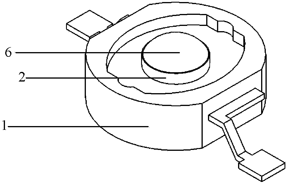
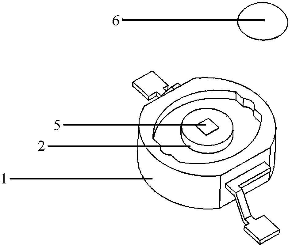
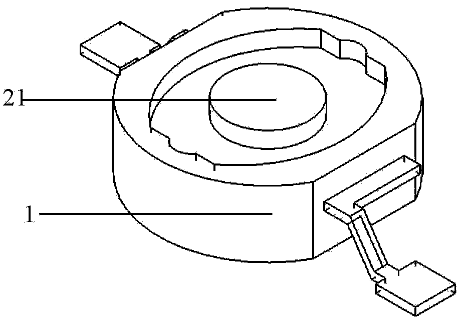
[0074] refer to Figure 5 , Figure 6 , Figure 7 , Figure 8 , Figure 5 It is a three-dimensional schematic diagram of the LED packaging structure provided by Embodiment 1 of the present invention, Figure 6 It is an exploded view of the LED packaging structure provided by Embodiment 1 of the present invention, Figure 7 It is a three-dimensional schematic diagram of the LED packaging structure bracket body provided by Embodiment 1 of the present invention, Figure 8 It is a partially enlarged schematic diagram of the substrate in the LED packaging structure provided by Embodiment 1 of the present invention; it can be seen from the figure that the LED packaging structure provided by Embodiment 1 includes a bracket body 1, a substrate 2, an LED chip 5, and a fluorescent glue 6 There is a base 2 in the bracket body 1, the base 2 is made of metal (such as aluminum, copper) or ceramic material, the base 2 has a reflective structure 3 and a chip groove 4, the chip groove 4 i...

Embodiment 2

[0078] refer to Figure 13 , Figure 14 , Figure 15 , Figure 16 , Figure 13 It is a three-dimensional schematic diagram of the LED packaging structure provided by Embodiment 2 of the present invention, Figure 14 It is an exploded view of the LED packaging structure provided by Embodiment 2 of the present invention, Figure 15 It is a three-dimensional schematic diagram of the bracket body of the LED packaging structure provided by Embodiment 2 of the present invention, Figure 16 It is a partially enlarged schematic diagram of the substrate in the LED packaging structure provided by Embodiment 2 of the present invention; it can be seen from the figure that the LED packaging structure provided by Embodiment 2 includes a bracket body 1, a substrate 2, an LED chip 5, and a fluorescent glue 6 There is a base 2 in the bracket body 1, the base 2 is made of metal (such as aluminum, copper) or ceramic material, the base 2 has a reflective structure 3 and a chip groove 4, the ...

Embodiment 3

[0082] refer to Figure 20 , Figure 21 , Figure 22 , Figure 23 , Figure 20 It is a three-dimensional schematic diagram of the LED packaging structure provided by Embodiment 3 of the present invention, Figure 21 It is an exploded view of the LED packaging structure provided by Embodiment 3 of the present invention, Figure 22 It is a three-dimensional schematic diagram of the bracket body of the LED packaging structure provided by Embodiment 3 of the present invention, Figure 23 A partially enlarged schematic diagram of the substrate in the LED packaging structure provided by Embodiment 3 of the present invention; it can be seen from the figure that the LED packaging structure provided by Embodiment 3 includes a bracket body 1, a substrate 2, an LED chip 5, and a fluorescent glue 6 There is a base 2 in the bracket body 1, the base 2 is made of metal (such as aluminum, copper) or ceramic material, the base 2 has a reflective structure 3 and a chip groove 4, the chip g...


PUM


Abstract

The invention discloses an LED packaging substrate and an LED packaging structure adopting the substrate. The substrate in the invention is of metal (such as aluminum, copper) or ceramic material, an upper surface of the substrate is provided with a reflective structure and a chip slot, the reflective structure of the upper surface of the substrate is reflected as two segments of disconnected arc-shaped structures in a top view, the chip slot is used for placing an LED chip and filling fluorescent glue, and the reflective structure is located outside the chip slot; and the reflective structure of the upper surface of the substrate adjusts the direction of a portion of light through reflection, further adjusts spatial light intensity distribution, thereby decreasing beam angles of some directions, or enabling light to lean to one side, and light color uniformity of light spots can be improved.

Description

technical field [0001] The invention relates to the technical field of LED lighting, in particular to an LED package base and an LED package structure using the base. Background technique [0002] In recent years, with the rise of the concept of energy saving worldwide, the general lighting technology using white LEDs has developed rapidly, especially in the field of street lighting applications for outdoor lighting. The light source efficiency of white LED single lamps using blue LED chips as excitation sources The laboratory level has reached more than 200lm / W, and the general application level in the market has also exceeded 120lm / W, which has far exceeded the light efficiency of ordinary energy-saving lamps. As white LED technology is becoming more and more popular in the general lighting market The application of white light LED devices has higher and higher requirements for luminous efficiency and luminous quality. [0003] LED packaging structure in the prior art (se...

Claims


Application Information

Patent Timeline
Patent Type & Authority Applications(China)
IPC IPC(8): H01L33/48H01L33/60
CPCH01L33/483H01L33/60
Inventor 刘凯王慧东赵乐令冯伟张彦伟孙夕庆
Owner ADVANCED OPTRONIC DEVICES CHINA
Why Eureka
Try Eureka