A siw-based hermetic packaging structure for millimeter-wave chips

A packaging structure and millimeter-wave technology, which is applied in waveguides, electrical components, waveguide-type devices, etc., can solve the problems of large millimeter-wave losses and achieve great economic benefits, low cost, and easy processing

Active Publication Date: 2016-06-08
THE 13TH RES INST OF CHINA ELECTRONICS TECH GRP CORP
View PDF4 Cites 0 Cited by
  • Summary
  • Abstract
  • Description
  • Claims
  • Application Information

AI Technical Summary

Problems solved by technology

[0004] The technical problem to be solved by the present invention is to provide an SIW-based millimeter-wave chip hermetic packaging structure, which can overcome the defect of large millimeter-wave loss in ceramic package packaging in the prior art, and solve the problem of millimeter-wave monolithic integration. The circuit, which is the hermetic packaging of the power amplifier circuit, the invention can realize the airtight packaging of the low-cost, high-performance millimeter-wave chip, the process is simple, easy to process, and can bring greater economic benefits

Method used


Image

  • A siw-based hermetic packaging structure for millimeter-wave chips

Examples


Embodiment Construction

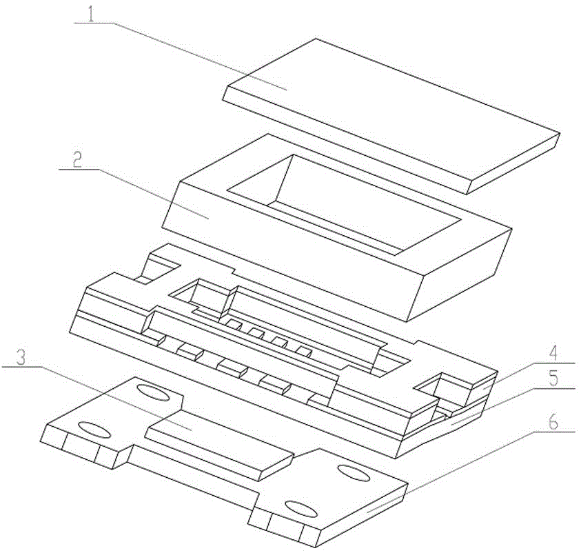
[0019] Depend on figure 1 It can be seen from the figure that an SIW-based millimeter-wave chip hermetic packaging structure includes a base 6 , an LTCC substrate, a sealing ring 2 and a cover plate 1 which are sealed and connected sequentially from bottom to top.

[0020] The base 6 of the package is made of tungsten copper material. The thermal expansion coefficient of tungsten copper is the same as that of GaAs and other microwave integrated circuits, and the heat dissipation performance is relatively good, which can improve the heat conduction and thermal matching of the power amplifier circuit of the millimeter wave chip, and improve the power amplifier circuit. Efficiency, improve the reliability of millimeter wave chip work.

[0021] The center of the base 6 is provided with a boss 3 for sintering millimeter-wave chips, and the height of the base 6 other than the boss 3 is lower than that of the boss 3; mounting holes can also be provided around the base 6 for easy inst...


PUM


Abstract

The invention discloses a millimeter wave chip gas tightness packaging structure based on an SIW and belongs to the technical field of semiconductors. The millimeter wave chip gas tightness packaging structure based on the SIW comprises a base, an LTCC substrate, a sealing ring, a cover plate and a center boss of the base, wherein the base, the LTCC substrate, the sealing ring and the cover plate are sequentially connected in a sealing mode from top to bottom. The LTC substrate is arranged around the periphery of the boss and is composed of a signal transmission layer and a ceramic cavity layer which are arranged in an up-and-down mode, and the upper surfaces of the signal transmission layer and the upper surface of the ceramic cavity layer are coated with metal layers. One pair of two opposite sides of the signal transmission layer are of SIW structures transmitting radio frequency signals. The sealing ring is located on the upper portion of the ceramic cavity layer, and the cover plate is located above the sealing ring. The millimeter wave chip gas tightness packaging structure overcomes the defects that a ceramic pipe shell is packaged into millimeter waves and losses are large in the prior art, in addition, the application frequency the higher, the packaging losses are fewer, and the sealing problem of a millimeter wave band microwave monolithic integrated circuit, and especially a power amplifier circuit is solved. Importantly, the millimeter wave chip gas tightness packaging structure is simple in achieving technology, convenient to machine, capable of indirectly bringing large economic benefits and good in promotional prospect.

Description

technical field [0001] The invention belongs to the technical field of semiconductors. Background technique [0002] For the packaging of microwave integrated circuits, the frequency response characteristics often limit the application frequency range of the circuit, and special consideration should be given to the design of radio frequency performance. The higher the microwave operating frequency, the more significant the impact of package parasitic parameters on the circuit. In order to reduce the impact of parasitic on performance, in millimeter-wave modules and components, monolithic integrated circuits are generally applied in the form of bare chips. In order to ensure airtightness, the entire module can only be sealed by soldering or laser sealing. Due to the generally large size of the components and the limitations of the process, the stability of these two sealing technologies is not easy to guarantee, and it is difficult to achieve hermetic packaging. However, th...

Claims


Application Information

Patent Timeline
Patent Type & Authority Patents(China)
IPC IPC(8): H01P3/16
Inventor 王绍东高艳红吴洪江
Owner THE 13TH RES INST OF CHINA ELECTRONICS TECH GRP CORP
Why Eureka
Try Eureka