Array substrate, display panel and display device

An array substrate and array technology, applied in the field of liquid crystal display, can solve the problem of increasing hardware cost, and achieve the effect of reducing peak power and saving hardware cost

Active Publication Date: 2014-07-09
BOE TECH GRP CO LTD +1
View PDF4 Cites 9 Cited by
  • Summary
  • Abstract
  • Description
  • Claims
  • Application Information

AI Technical Summary

Problems solved by technology

[0004] However, the time-sharing scanning adopted in the prior art is completed through the separation of odd and even rows, requiring more integrated circuit elements (Integrate Circuit, IC) for driving.
It can be seen that although the peak power during gate scanning is reduced to a certain extent, the hardware cost is greatly increased

Method used


Image

  • Array substrate, display panel and display device
  • Array substrate, display panel and display device
  • Array substrate, display panel and display device

Examples


Embodiment Construction

[0041] The implementation process of the embodiment of the present invention will be described in detail below in conjunction with the accompanying drawings. It should be noted that the same or similar reference numerals represent the same or similar elements or elements having the same or similar functions throughout. The embodiments described below by referring to the figures are exemplary only for explaining the present invention and should not be construed as limiting the present invention. Apparently, the described embodiments are only some of the embodiments of the present invention, but not all of them. Based on the embodiments of the present invention, all other embodiments obtained by persons of ordinary skill in the art without making creative efforts belong to the protection scope of the present invention.

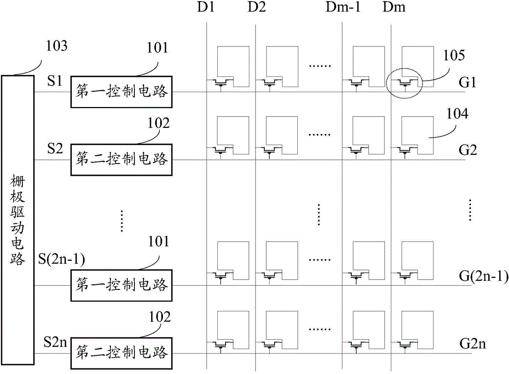
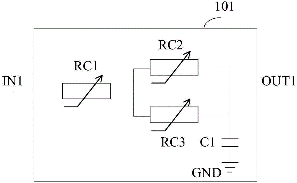
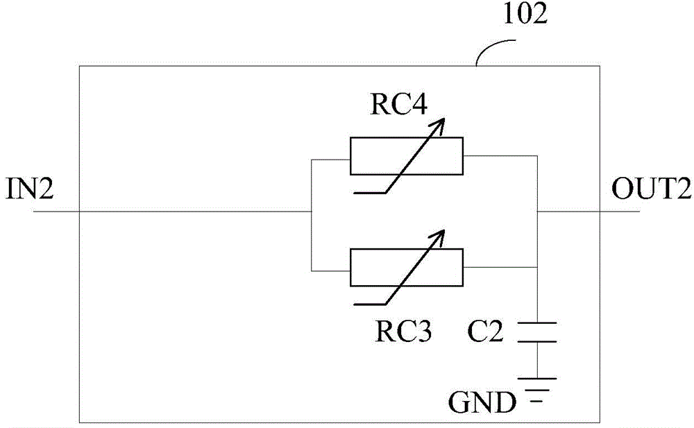
[0042] see figure 1 , the embodiment of the present invention provides an array substrate, including a pixel unit 104 array composed of a plurality of pixel u...


PUM


Abstract

The invention discloses an array substrate, a display panel and a display device. The array substrate comprises a plurality of first control circuits, a plurality of second control circuits and a grid driving circuit. The grid driving circuit is electrically connected with input ends of the various first control circuits and input ends of the various second control circuits; all grid lines are divided into a first grid line group and a second grid line group, an output end of each first control circuit is electrically connected with grids of a TFT (thin film transistor) row by the corresponding grid line in the first grid line group, and an output end of each second control circuit is electrically connected with grids of a TFT row by the corresponding grid line in the second grid line group; the grid driving circuit is used for being alternately synchronized with frames to alternately provide first level signals and second level signals and providing third level signals, the first level signals and the second level signals are used for turning on TFTs, and the third level signals are used for turning off the TFTs; the first level signals and the second level signals can be selectively transmitted through the first control circuits and the second control circuits. The array substrate, the display panel and the display device have the advantage that the purpose of reducing peak power during grid scanning can be achieved without increase of driving chips or complicated connecting lines.

Description

technical field [0001] The present invention relates to the technical field of liquid crystal display, in particular to an array substrate, a display panel and a display device. Background technique [0002] When a liquid crystal display is performing grid scanning, it usually scans from one end to the other end sequentially. During this scanning process, the peak power is high, which tends to generate more heat and affect the life of the liquid crystal display. [0003] In the prior art, the odd and even rows are usually separated and wired on the array substrate, and the driving chip is added to realize the time-sharing scanning of the thin film transistors (Thin Film Transistor, TFT) in the odd and even rows, which can reduce the peak power and reduce the generation of heat. Extend the life of LCD monitors. [0004] However, the time-division scanning adopted in the prior art needs to add more integrated circuit components (Integrate Circuit, IC) for driving because it i...

Claims


Application Information

Patent Timeline
Patent Type & Authority Applications(China)
IPC IPC(8): G02F1/1362G02F1/1368G09G3/36
Inventor 张春兵
Owner BOE TECH GRP CO LTD
Why Eureka
Try Eureka