Touch screen, touch screen manufacturing method and display device

A touch screen and touch technology, applied in instruments, electrical digital data processing, input/output process of data processing, etc., can solve the problems of contamination chambers, surface protrusions and depressions, poor process, etc., so as to avoid contamination chambers. room, the effect of ensuring quality

Inactive Publication Date: 2014-07-09
BOE TECH GRP CO LTD
View PDF3 Cites 8 Cited by
  • Summary
  • Abstract
  • Description
  • Claims
  • Application Information

AI Technical Summary

Problems solved by technology

Since the material of the shielding layer 02 contains a resin material, when the base substrate 01 formed with the shielding layer 02 is bombarded by plasma (plasma) in the sputtering chamber, other substances will be released, thus contaminating the chamber
In addition, when the plasma bombards the surface of the shielding layer 02, it will also cause uneven defects such as protrusions and depressions on the surface of the shielding layer 02, which will affect the flatness of the subsequent film layer and cause problems such as poor craftsmanship.

Method used


Image

  • Touch screen, touch screen manufacturing method and display device
  • Touch screen, touch screen manufacturing method and display device
  • Touch screen, touch screen manufacturing method and display device

Examples


example 1

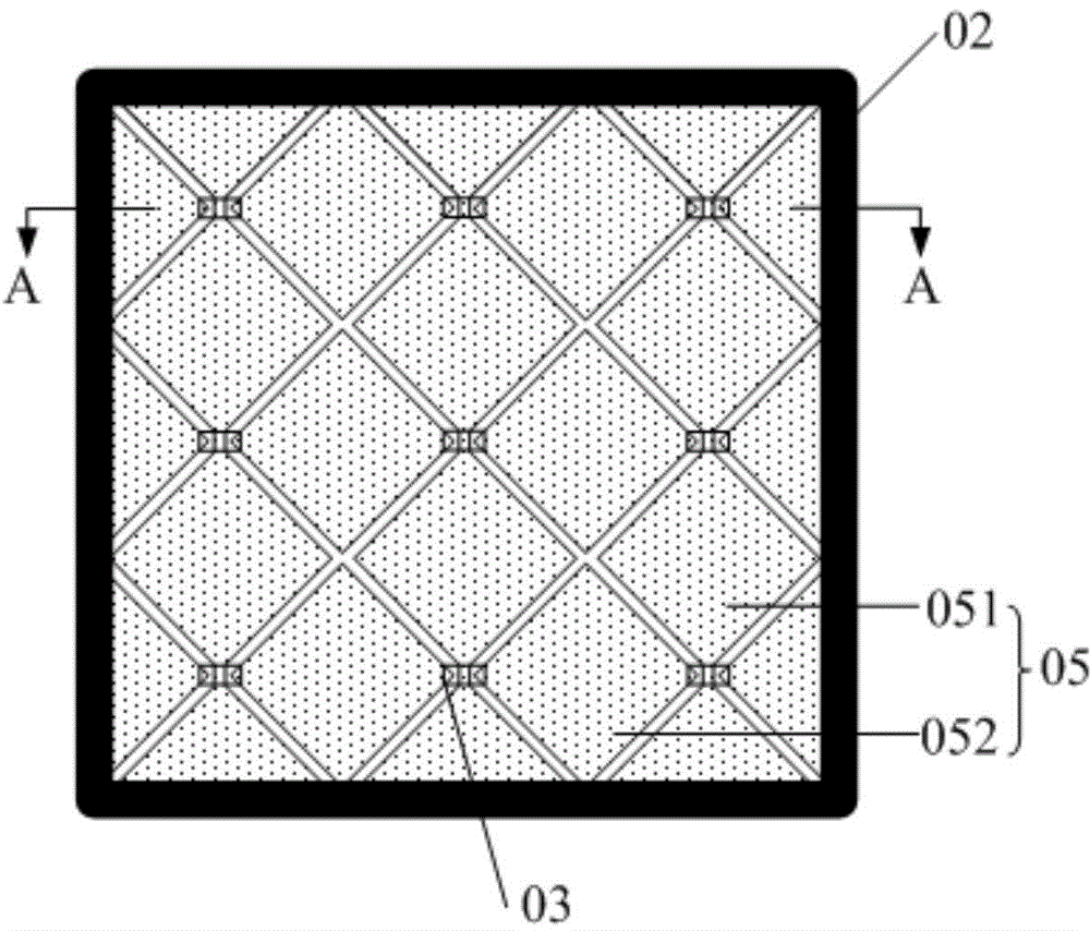
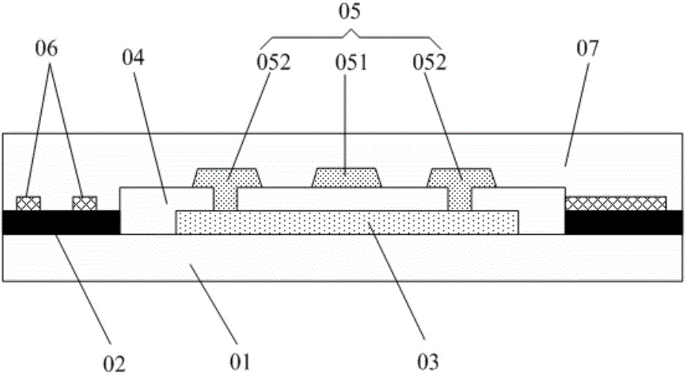
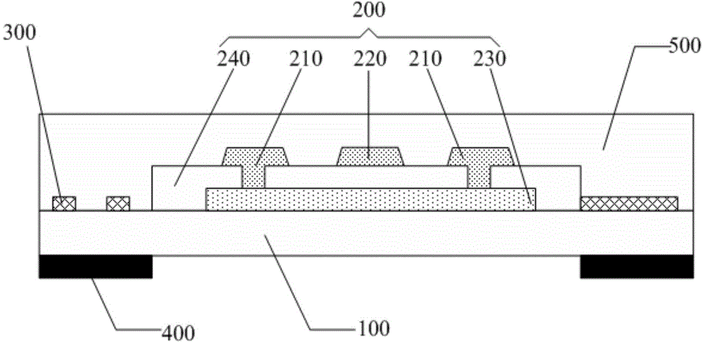
[0051] Specifically, in production such as image 3 In the case of the touch screen shown in the figure, the pattern including the shielding layer 400 is first formed on one side of the base substrate 100, then the base substrate 100 is turned over, and then peripheral wiring including electrical connections is formed on the other side of the base substrate 100 300 and the pattern of the touch control structure 200, wherein the touch control structure 200 includes touch sensing electrodes 210 and touch driving electrodes 220 arranged in the same layer, intersecting and insulated from each other, bridging the bridge between adjacent touch sensing electrodes 210 layer 230; and an insulating layer 240 between the bridging layer 230 and the touch sensing electrodes 210 and touch driving electrodes 220 arranged on the same layer; the touch screen manufacturing process, such as Figure 4 As shown, specifically, the following steps may be included:

[0052] S401, forming a pattern i...

example 2

[0067] in production as image 3 In the case of the touch screen shown in the figure, a pattern including electrically connected peripheral traces 300 and the touch structure 200 is first formed on one side of the base substrate 100, then the base substrate 100 is turned over, and then the other side of the base substrate 100 Forming a pattern including a shielding layer 400, wherein the touch structure 200 includes touch sensing electrodes 210 and touch driving electrodes 220 arranged in the same layer, intersecting and insulated from each other, bridging the bridging layer of adjacent touch sensing electrodes 210 230; and an insulating layer 240 between the bridging layer 230 and the touch sensing electrodes 210 and touch driving electrodes 220 arranged on the same layer; the touch screen manufacturing process, such as Figure 5 As shown, specifically, the following steps may be included:

[0068] S501, forming a pattern including an anti-reflection layer 600 on one side of...


PUM


Abstract

The invention discloses a touch screen, a touch screen manufacturing method and a display device. Since a touch structure and peripheral lines are positioned on one side of a substrate while a shielding layer is positioned on the other side of the substrate, namely the shielding layer and the touch structure are positioned on two sides of the substrate respectively, when the touch structure and the peripheral lines are made on the substrate of the touch screen by means of sputtering, and the shielding layer on the other side of the substrate can be protected from strafing of plasmas in a sputtering cavity so as to be prevented from contaminating the cavity. In addition, due to the fact that the shielding layer is positioned on the other side of the substrate, compared with the prior art in which the touch structure and the peripheral lines are formed on a film layer of the shielding layer, the touch screen, the touch screen manufacturing method and the display device have the advantages that the problem of unevenness of the touch structure resulted from unevenness of the shielding layer is avoided, and quality of the touch screen is guaranteed.

Description

technical field [0001] The invention relates to the field of touch technology, in particular to a touch screen, a manufacturing method and a display device. Background technique [0002] With the rapid development of display technology, touch screen panels (Touch Screen Panels) have gradually spread throughout people's lives. At present, touch screens can be divided into: resistive, capacitive, infrared, surface acoustic wave, electromagnetic, vibration induction, and frustrated total internal reflection optical induction, etc. according to their working principles. Among them, the capacitive touch screen is sought after by the industry as a new favorite due to its unique touch principle, high sensitivity, long life, high light transmittance and other advantages. [0003] The single-chip (OGS, One Glass Solution) touch module that is widely used at present is to directly form a single-layer touch conductive film and sensor on the substrate, such as Figure 1a with Figure ...

Claims


Application Information

Patent Timeline
Patent Type & Authority Applications(China)
IPC IPC(8): G06F3/041
CPCG06F3/0445G06F3/0446G06F2203/04111
Inventor 齐永莲徐传祥舒适
Owner BOE TECH GRP CO LTD
Why Eureka
Try Eureka