
Color film substrate, manufacturing method thereof and display device

The technology of a color filter substrate and a manufacturing method is applied in the display field and can solve the problems of reducing the aperture ratio of the display device and reducing the resolution of the display device by distance.

Inactive Publication Date: 2014-07-23
BOE TECH GRP CO LTD +1
View PDF4 Cites 30 Cited by
  • Summary
  • Abstract
  • Description
  • Claims
  • Application Information

AI Technical Summary

Problems solved by technology

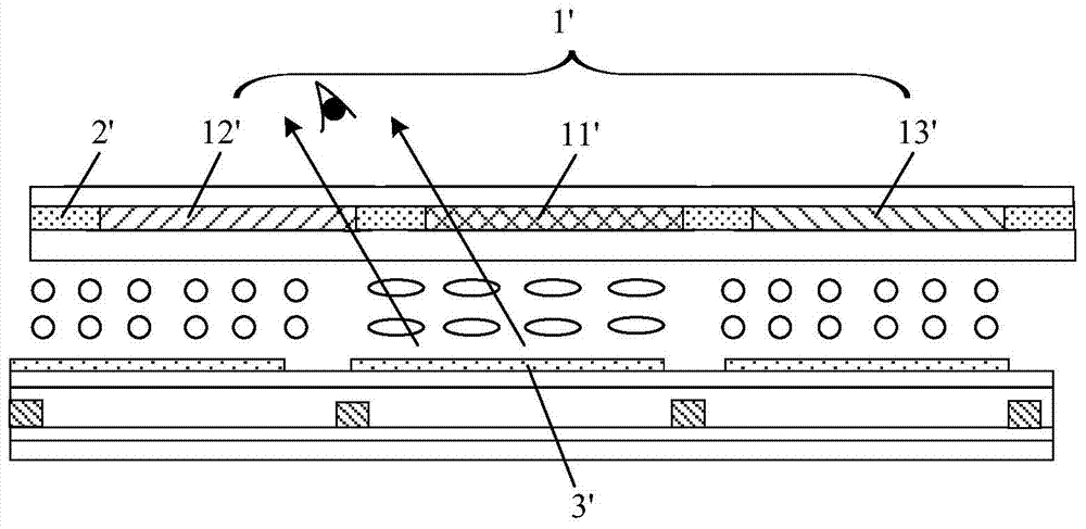
The inventors have found that increasing the lateral width of the black matrix 2' will reduce the aperture ratio of the display device; increasing the distance between the pixel electrodes 3' in two adjacent pixel units will reduce the resolution of the display device

Method used


Image

  • Color film substrate, manufacturing method thereof and display device
  • Color film substrate, manufacturing method thereof and display device
  • Color film substrate, manufacturing method thereof and display device

Examples


Embodiment 1

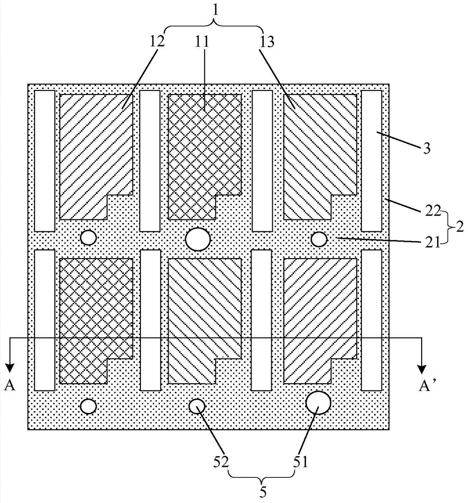
[0053] Embodiments of the present invention provide a figure 2 and image 3 The color filter substrate shown.

[0054] The color filter substrate includes a color filter layer 1, and the color filter layer 1 includes color filter units of at least two colors distributed in a matrix, and a black matrix 2 is arranged between adjacent color filter units. Specifically, the color filter layer 1 includes a red filter unit 11 , a green filter unit 12 and a blue filter unit 13 . The color filter units of different colors in the color filter layer 1 are generally made of color photosensitive resins of corresponding colors.

[0055] Further, the color filter substrate further includes a light-shielding protrusion 3 located in the area where the black matrix 2 is located, so as to prevent color mixing between color filter units of different colors.

[0056] It should be noted that the light-blocking protrusion 3 must be made of opaque material, and the specific material can be select...

Embodiment 2

[0068] The embodiment of the present invention provides a method for manufacturing a color filter substrate, such as Image 6 As shown, the production method includes:

[0069] Step S601 , forming a pattern including a color filter layer, a black matrix, and light-shielding protrusions on a base substrate.

[0070] Wherein, the color filter layer 1 includes color filter units of at least two colors distributed in a matrix.

[0071] The black matrix 2 is located between adjacent color filter units.

[0072] The light blocking protrusion 3 is located in the area where the black matrix 2 is located to prevent color mixing between color filter units of different colors.

[0073] Optionally, the lateral width of the light blocking protrusion 3 is less than or equal to the lateral width of the black matrix 2 .

[0074] Optionally, the longitudinal length of the light blocking protrusion 3 is greater than or equal to the longitudinal maximum length of the color filter layer 1 .

...


PUM


Abstract

The embodiment of the invention discloses a color film substrate, a manufacturing method of the color film substrate and a display device, and relates to the technical field of display. Under the condition of ensuring that the display device has the high aperture opening ratio and resolution ratio, the color mixing phenomenon of the display device is prevented. The color film substrate comprises a color filter layer, the color filer layer comprises color filer units of at least two colors, the color filer units are distributed in a matrix mode, a black matrix is arranged between every two adjacent color filter units, and the color film substrate further comprises light blocking protrusions which are arranged in an area where the blade matrixes are located, so that color mixing between the color filter units of different colors is prevented.

Description

technical field [0001] The invention relates to the field of display technology, in particular to a color filter substrate, a manufacturing method thereof, and a display device. Background technique [0002] A display device generally includes an array substrate and a color filter substrate. Specifically, pixel units arranged in an array are arranged on the array substrate, and the pixel units include pixel electrodes. Refer to figure 1 As shown, the color filter substrate is provided with a color filter layer 1', and the color filter layer 1' includes a red filter unit 11', a green filter unit 12' and a blue filter unit 13', and the adjacent color filter A black matrix 2' is arranged between the light units. The manufacturing process of the display panel includes steps such as manufacturing an array substrate, manufacturing a color filter substrate, and boxing the array substrate and the color filter substrate. [0003] Array substrates and color filter substrates are pr...

Claims


Application Information

Patent Timeline
Patent Type & Authority Applications(China)
IPC IPC(8): G02F1/1335G02F1/1333
CPCG02B5/201G02F1/133512G02F1/133516G02F1/13394Y10T29/49826
Inventor 杨小飞樊浩原莫再隆石天雷朴承翊
Owner BOE TECH GRP CO LTD
Learn More