Display pixel configuration structure, display panel and preparation method of display panel

A technology for displaying pixels and pixels, which is used in semiconductor/solid-state device manufacturing, semiconductor devices, electrical components, etc., can solve the problems of high difficulty in mask production and easy color mixing of vapor-deposited sub-pixels, so as to reduce the difficulty of production and avoid color mixing. Effect

Active Publication Date: 2017-07-25
WUHAN TIANMA MICRO ELECTRONICS CO LTD
View PDF3 Cites 19 Cited by
  • Summary
  • Abstract
  • Description
  • Claims
  • Application Information

AI Technical Summary

Problems solved by technology

[0007] In view of this, the present invention provides a display pixel arrangement structure, a display panel and a method for preparing the display panel, which solves the difficulty in making the mask for evaporating sub-pixels in the prior art and the difficulty in the process of evaporating sub-pixels. Technical problems of easy color mixing

Method used


Image

  • Display pixel configuration structure, display panel and preparation method of display panel
  • Display pixel configuration structure, display panel and preparation method of display panel
  • Display pixel configuration structure, display panel and preparation method of display panel

Examples


Embodiment

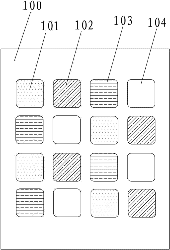
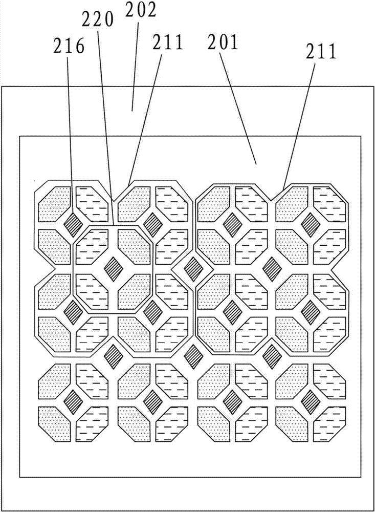
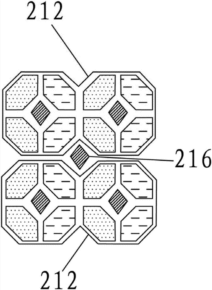
[0050] Such as Figure 2 to Figure 7 as shown, figure 2 It is a schematic diagram of a display pixel arrangement structure in a display panel provided in this embodiment; the display panel here may be an organic display panel or an inorganic display panel; image 3 for figure 2 Schematic diagram of the structure of a pixel group in , a pixel group is equivalent to a display pixel area; Figure 4 for image 3 Schematic diagram of the structure of a pixel group pair in ; Figure 5 for Figure 4 Schematic diagram of the structure of a pixel group in ; Figure 6 for Figure 5 Schematic diagram of the structure of the first sub-pixel pair; Figure 7 for Figure 5 Schematic diagram of the structure of the second sub-pixel pair in . The display panel includes a display area 201 and a non-display area 202 surrounding the display area. The display pixel arrangement structure in the display area 201 includes: a pixel group 211 arranged in an array, and the pixel group 211 inc...


PUM


Abstract

The invention discloses a display pixel configuration structure. The display pixel configuration structure comprises a pixel crowd arranged in an array, wherein the pixel crowd comprises two pixel group pairs arranged oppositely, and each pixel crowd pair comprises two adjacent pixel groups; each pixel group comprises a first sub-pixel pair and a second sub-pixel arranged oppositely and a third sub-pixel positioned at the central position between the first sub-pixel pair and the second sub-pixel pair, wherein in the pixel group, the first sub-pixel pair and the second sub-pixel pair are arranged along a row direction respectively, or the first sub-pixel pair and the second sub-pixel pair are arranged along a line direction respectively; the third sub-pixel is arranged at the central position between the adjacent pixel groups; the third sub-pixel is arranged at the central position among four pixel groups, and each third sub-pixel is adjacent to two first sub-pixels and two second sub-pixels respectively. According to the display pixel configuration structure, the manufacturing difficulty of a mask plate is reduced, and the pixel resolution ratio is improved.

Description

technical field [0001] The present invention relates to the technical field of display, and more specifically, to a display pixel arrangement structure, a display panel and a method for preparing the display panel. Background technique [0002] In the panel display technology, the organic light-emitting diode (Organic Light-Emitting Diode, OLED) display technology is different from the traditional liquid crystal display (LCD) technology. The substrate has many advantages such as fast response speed, wide viewing angle, rich colors, low power consumption and high and low temperature resistance, and has become a key development technology in the current industry. OLED display panel, after the driving circuit receives the external signal, controls the working state of the thin film transistor to supply the ideal potential preset by the reflective anode, so that a potential difference is formed between the reflective anode and the semi-transparent cathode, and the electrons and ...

Claims


Application Information

Patent Timeline
Patent Type & Authority Applications(China)
IPC IPC(8): H01L27/32H01L51/56
CPCH10K59/35H10K59/353H10K71/164H10K71/166H10K71/00
Inventor 王永志熊志勇
Owner WUHAN TIANMA MICRO ELECTRONICS CO LTD
Why Eureka
Try Eureka