Electroluminescent display device

a display device and electroluminescent technology, applied in non-linear optics, instruments, optics, etc., can solve problems such as color mixture problems, optical efficiency degradation, and pixel pitch reduction, and achieve the effect of improving optical efficiency and preventing color mixtur

Active Publication Date: 2019-06-20
LG DISPLAY CO LTD
View PDF5 Cites 18 Cited by
  • Summary
  • Abstract
  • Description
  • Claims
  • Application Information

AI Technical Summary

Benefits of technology

[0008]In addition, the present disclosure is to provide an electroluminescent display device that is capable of improving optical efficiency and adjusting a path of light output to the outside while preventing color mixture.

Problems solved by technology

Recently, as the size of substrates has been increased and display devices have evolved to have a high resolution, a pixel pitch has been decreased, and optical efficiency degradation and color mixture have been problems.

Method used


Image

  • Electroluminescent display device
  • Electroluminescent display device
  • Electroluminescent display device

Examples


Embodiment Construction

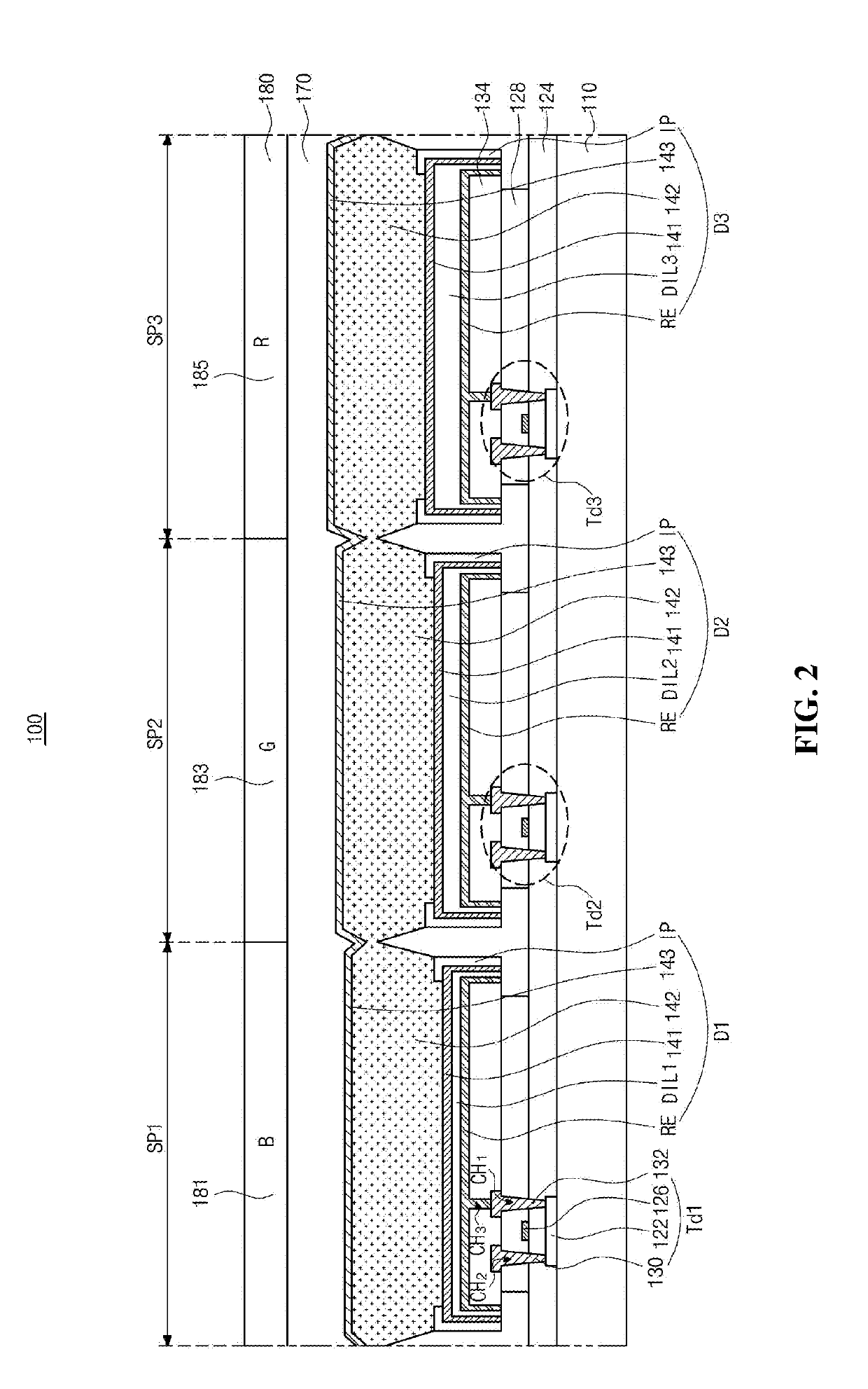
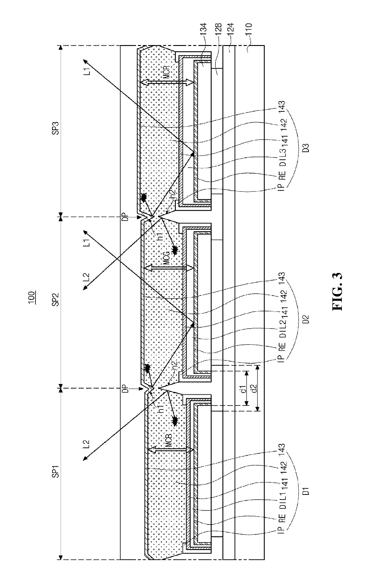
[0021]Hereinafter, exemplary aspects of the present disclosure will be described with reference to the accompanying drawings. Wherever possible, the same reference numbers will be used throughout the drawings to refer to the same or like parts.

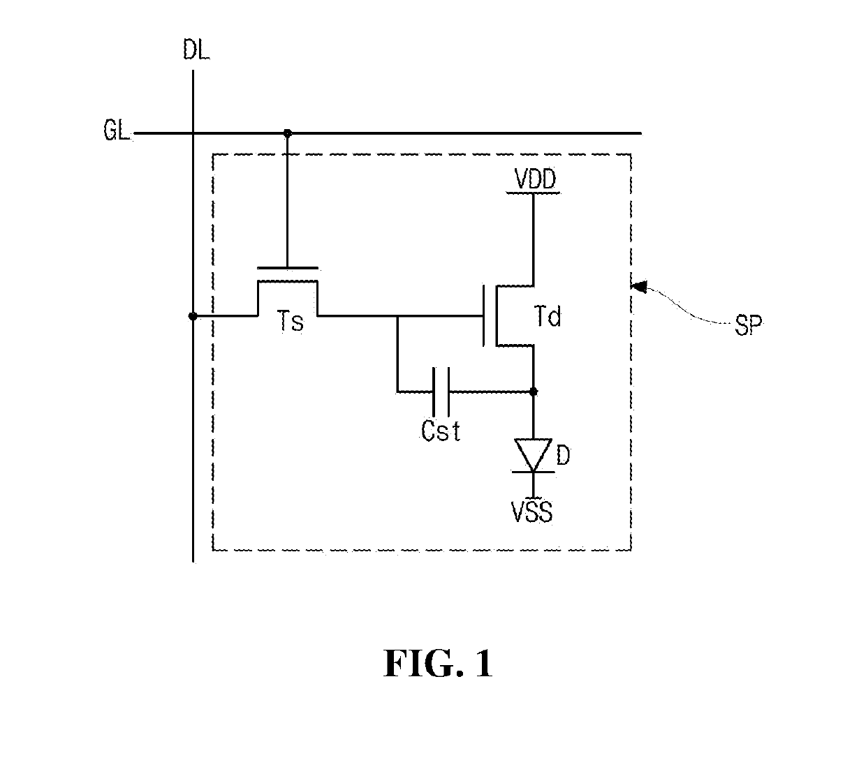
[0022]FIG. 1 is a circuit diagram illustrating a single sub-pixel region of an electroluminescent display device according the present disclosure.

[0023]As illustrated in FIG. 1, the electroluminescent display device according to an aspect of the present disclosure includes a gate line GL, a data line DL, a switching thin film transistor Ts, a driving thin film transistor Td, a storage capacitor Cst and a light-emitting diode D. The gate line GL and the data line DL cross each other and define a sub-pixel region SP. The switching thin film transistor Ts, the driving thin film transistor Td, the storage capacitor Cst and the light-emitting diode D are formed in the sub-pixel region SP.

[0024]More specifically, a gate electrode of the switching th...


PUM

PropertyMeasurementUnit
voltageaaaaaaaaaa
thicknessaaaaaaaaaa
shapeaaaaaaaaaa

Abstract

An electroluminescent display device includes a substrate including first, second, and third sub-pixel regions; an interlayer insulating layer and a passivation layer each separately disposed at the first, second, and third sub-pixel regions on the substrate; a reflective electrode disposed on the passivation layer of each of the first, second, and third sub-pixel regions; first, second, and third dielectric layers disposed corresponding to the first, second, and third sub-pixel regions, respectively, on the reflective electrode; a first electrode disposed on each of the first, second, and third dielectric layers; an insulating pattern covering an edge of the first electrode; a light-emitting layer disposed on the first electrode and the insulating pattern and substantially all over the substrate including the first, second, and third sub-pixel regions; and a second electrode disposed on the light-emitting layer, wherein the first, second, and third dielectric layers have different thicknesses.

Description

CROSS-REFERENCE TO RELATED APPLICATION[0001]This application claims the benefit under 35 U.S.C. § 119(a) of Korean Patent Application No. 10-2017-0173903, filed on Dec. 18, 2017, in the Korean Intellectual Property Office, which is incorporated herein by reference in its entirety.BACKGROUNDField of the Disclosure[0002]The present disclosure relates to an electroluminescent display device, and more particularly, to an electroluminescent display device capable of adjusting an optical path while improving optical efficiency and preventing color mixture among sub-pixels.Description of the Background[0003]In recent years, flat panel displays having excellent characteristics such as being thin, lightweight, and having low power consumption have been widely developed and applied to various fields.[0004]Among the flat panel displays, an electroluminescent display device is a device in which electrical charge carriers are injected into a light-emitting layer formed between a cathode, which i...

Claims


Application Information

Patent Timeline
Patent Type & Authority Applications(United States)
IPC IPC(8): H01L27/32G02F1/1335H01L51/52G03H1/02
CPCH01L27/3209G02F1/133526H01L27/322H01L51/5206H01L51/5221H01L51/5237G03H1/02G03H2001/0216H10K59/35H10K59/122H10K59/124H10K59/121H10K50/80H10K50/805H10K59/38H10K50/81H10K50/852H10K50/856H10K2102/3026H01L27/156H01L33/405H01L33/38H01L33/58H10K59/32H10K50/82H10K50/84
Inventor BANG, HYUNG-SEOKPARK, JI-YEONPARK, HAN-SUNLIM, HYEONG-JUN
Owner LG DISPLAY CO LTD
Why Eureka
Try Eureka