Diamond sensors, detectors, and quantum devices

a detector and diamond technology, applied in the field of diamond sensors, detectors and quantum devices, can solve the problems of insufficient to achieve very high decoherence times, low decoherence time of isolated quantum spin defects, and reduced number, so as to reduce the decoherence time, reduce the number of quantum spin defects, and reduce the optical absorption of synthetic diamond materials

Active Publication Date: 2014-06-24
ELEMENT SIX LTD
View PDF7 Cites 63 Cited by
  • Summary
  • Abstract
  • Description
  • Claims
  • Application Information

AI Technical Summary

Benefits of technology

[0021]The present inventors have realized that it is problematic to introduce a high concentration of quantum spin defects into synthetic CVD diamond material without detrimentally affecting the optical properties of the material and the decoherence time of the quantum spin defects. Furthermore, the present inventors have realized that bulk samples of synthetic HPHT diamond material have a concentration of quantum spin defects, such as NV− defects, which is too high to optically isolate individual defects and that the high number of quantum spin defects leads to a reduction in decoherence time. The present inventors have found that if a synthetic diamond material having a relatively high concentration of quantum spin defects is processed to form a very thin layer of such material, it is possible for individual quantum spin defects to be optically isolated. Furthermore, by processing the material to be very thin then optical absorption within the synthetic diamond material is reduced thus increasing the efficiency of excitation of the quantum spin defects and light collection therefrom. In this way, synthetic diamond material which was not previously suitable for quantum spin applications may be processed into a form which is suitable for such applications. For example, the nitrogen concentration and film thickness of synthetic diamond material can be balanced so that quantum spin defects are optically isolated and have good optical efficiency in terms of excitation and light collection. This may be particularly useful for synthetic HPHT diamond material where thicker layers of material have a defect concentration which is too high to optically isolate individual quantum spin defects.
[0025]While improved values for the product of the quantum spin defect concentration and the decoherence time T2 of the quantum spin defects can be achieved by controlling the concentration of quantum spin defects and the concentration of other point defects as previously described, for thin plates of material it has also been found that surface termination groups can adversely interact with nearby quantum spin defects thus reducing the value of the product by reducing T2. This is particularly problematic for thin plates of diamond material which have a large surface area to volume ratio with a large number of quantum spin defects located relatively close to the surface of the material. As such, in order to increase the product of the quantum spin defect concentration and the decoherence time T2 of the quantum spin defects it is also considered necessary to control the surface termination of the thin plate of diamond material. In particular, it is considered advantageous to treat the plate of diamond material to provide surface termination species which have zero nuclear spin or zero electron spin, preferably both zero nuclear spin and zero electron spin. An example of such a species is 16O.

Problems solved by technology

However, it has been found that while balancing quantum spin defect concentration and film thickness in this manner can result in optically isolated quantum spin defects, the decoherence time T2 of the isolated quantum spin defects is still too low for many sensing and quantum processing applications.
However, for thin plates of material it has been found that this is still insufficient to achieve very high decoherence times.
However, while this will increase the sensitivity of each individual quantum spin defect, a reduction in the number of quantum spin defects will reduce the overall sensitivity of the material.

Method used


Image

  • Diamond sensors, detectors, and quantum devices
  • Diamond sensors, detectors, and quantum devices
  • Diamond sensors, detectors, and quantum devices

Examples


example

Preparation and Mounting of Thin Film

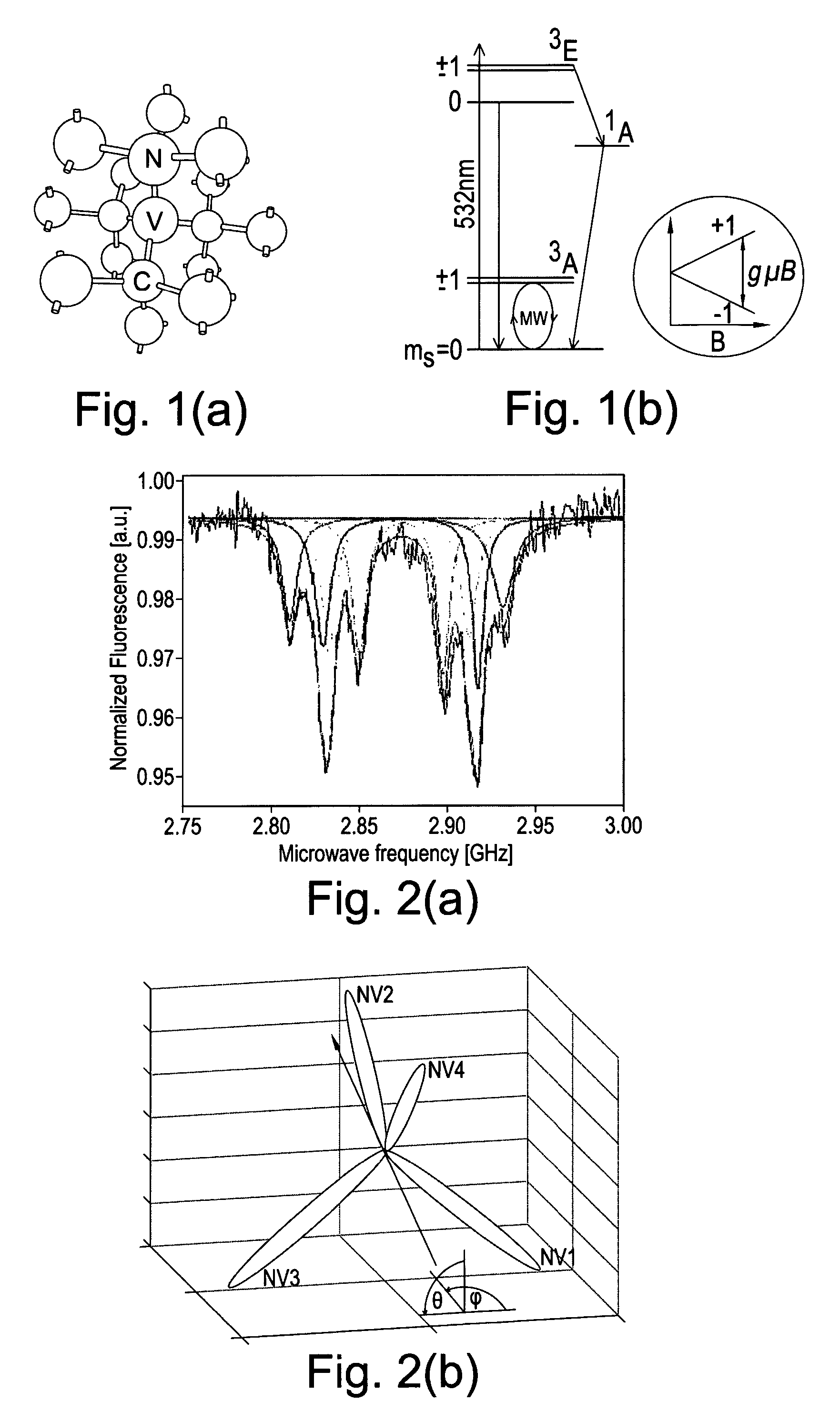
[0103]A type 1b synthetic HPHT diamond containing a nitrogen concentration of [N]0) and negatively charged (NV−) nitrogen-vacancy defects were the only colour centres detected in the sample. In the HPHT bulk sample a high density of such defects were observed, and individual colour centres could not be resolved.

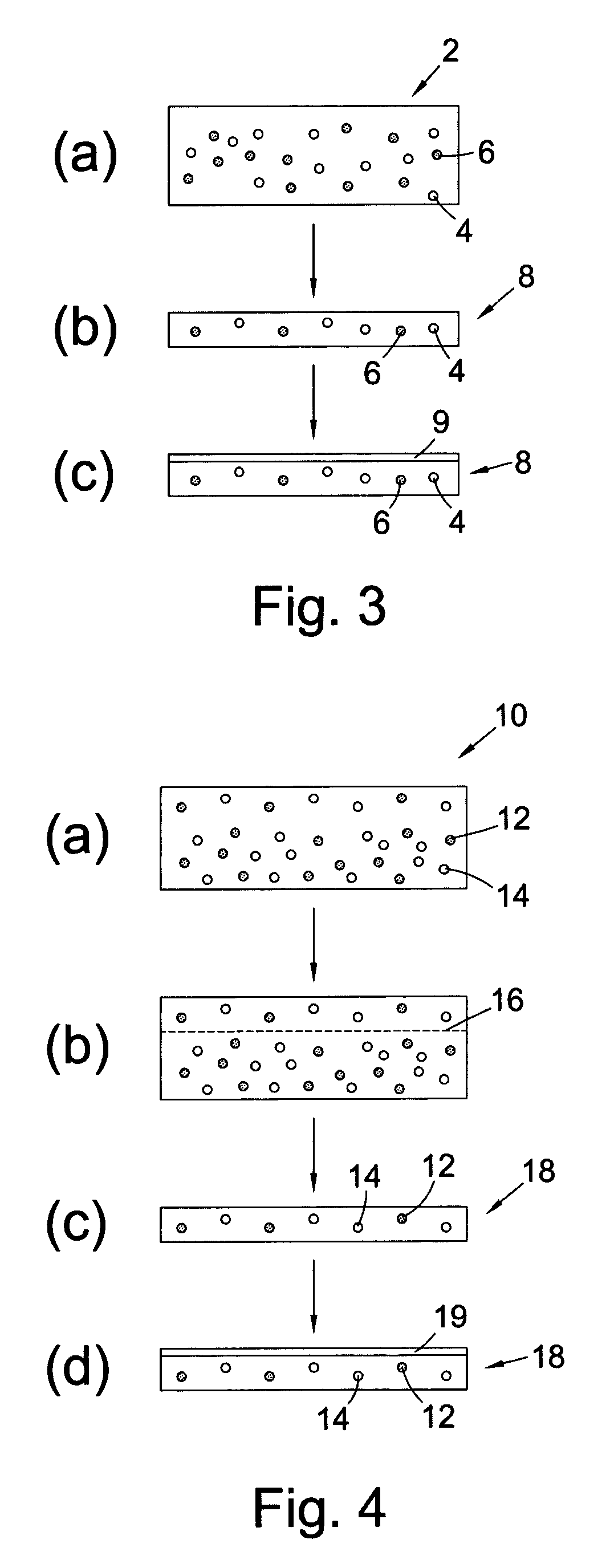
[0104]A film of 1 μm thickness was defined by implantation of He ions at an energy of 0.5 MeV and a fluence of approximately 5×10¹⁶ ions / cm2, followed by annealing in a forming gas (Ar, 4% H2) for one hour at 800° C. To grant access to the graphite layer, a focused-ion beam (FIB) of 30 keV Ga+ ions was used to drill 5 μm holes to a depth of 2 μm. The film was then undercut using a cycle of galvanic etches to remove the graphite layer. Once the graphite had been removed, a final clean in oxidizing acids removed any non-sp3 carbon. A further FIB milling process was then used to define an approximately square film of 60 to 80 μm side length.

[...


PUM

PropertyMeasurementUnit
thicknessaaaaaaaaaa
thicknessaaaaaaaaaa
thicknessaaaaaaaaaa

Abstract

A thin plate of synthetic single crystal diamond material, the thin plate of synthetic single crystal diamond material having: a thickness in a range 100 nm to 50 μιη; a concentration of quantum spin defects greater than 0.1 ppb (parts-per-billion); a concentration of point defects other than the quantum spin defects of below 200 ppm (parts-per-million); and wherein at least one major face of the thin plate of synthetic single crystal diamond material comprises surface termination species which have zero nuclear spin and / or zero electron spin.

Description

FIELD OF INVENTION[0001]The present invention relates to synthetic diamond material for use in sensing, detecting and quantum processing applications.BACKGROUND OF INVENTION[0002]Point defects in synthetic diamond material, particularly quantum spin defects and / or optically active defects, have been proposed for use in various sensing, detecting, and quantum processing applications including: magnetometers; spin resonance devices such as nuclear magnetic resonance (NMR) and electron spin resonance (ESR) devices; spin resonance imaging devices for magnetic resonance imaging (MRI); and quantum information processing devices such as for quantum computing.[0003]Many point defects have been studied in synthetic diamond material including: silicon containing defects such as silicon-vacancy defects (Si-V), silicon di-vacancy defects (Si-V2), silicon-vacancy-hydrogen defects (Si-V:H), silicon di-vacancy hydrogen defects (S-V2:H); nickel containing defect; chromium containing defects; and ni...

Claims


Application Information

Patent Timeline
Patent Type & Authority Patents(United States)
IPC IPC(8): C30B29/04
CPCH01L29/1602B82Y10/00C30B29/04C30B29/64C30B31/22C30B33/08G01N24/10G01R33/24G01R33/302G01R33/60G06N99/002H01L21/0405H01L29/157H01L29/167G06N10/00G01R33/12H01L21/02524
Inventor TWITCHEN, DANIEL JAMESMARKHAM, MATTHEW LEE
Owner ELEMENT SIX LTD
Why Eureka
Try Eureka