Surface plasmon excimer electrically-induced excitation source with medium-metal near field coupling structure and manufacturing method thereof

A surface plasmon and near-field coupling technology, which is applied in circuits, electrical components, semiconductor devices, etc., can solve the problems of small adjustable range of emission wavelength, small propagation distance of surface plasmons, and cumbersome preparation process. Achieve the effect of wide emission wavelength range, easy device integration, and simplified preparation process

Active Publication Date: 2015-01-07
TECHNICAL INST OF PHYSICS & CHEMISTRY - CHINESE ACAD OF SCI
View PDF3 Cites 16 Cited by
  • Summary
  • Abstract
  • Description
  • Claims
  • Application Information

AI Technical Summary

Problems solved by technology

However, the main disadvantage of this method is that there is a luminescent process in the middle and the photoelectric utilization efficiency is low.
[0008] In 2012, Stanford University’s P.Y.Fan et al. [Nano Lett., 12, 4943-4947, 2012] based on semiconductor nanowire LEDs to excite surface plasmons. Although it has advantages in waveguide coupling, it also has low quantum efficiency and luminescence. The defect of small wavelength tunable range
However, the device has some disadvantages
In terms of structure and principle, the excited surface plasmons propagate in the metal-dielectric-metal waveguide. Due to the strong mode confinement, the propagation distance of the surface plasmons is small, which affects the application of the device.
In terms of technology, it is necessary to bond the semiconductor epitaxial wafer to another silicon substrate, etch away the substrate of the original semiconductor epitaxial wafer, and then proceed to the device preparation process, which leads to a cumbersome preparation process, complicated process, and successful device preparation. Low rate, difficult to scale production

Method used


Image

  • Surface plasmon excimer electrically-induced excitation source with medium-metal near field coupling structure and manufacturing method thereof
  • Surface plasmon excimer electrically-induced excitation source with medium-metal near field coupling structure and manufacturing method thereof
  • Surface plasmon excimer electrically-induced excitation source with medium-metal near field coupling structure and manufacturing method thereof

Examples


Embodiment 1

[0041] Taking the GaAs-based semiconductor quantum well epitaxial material with a wavelength range of 0.5-1 μm as an example, a surface plasmon electric excitation source with a dielectric-metal near-field coupling structure and its Production Method.

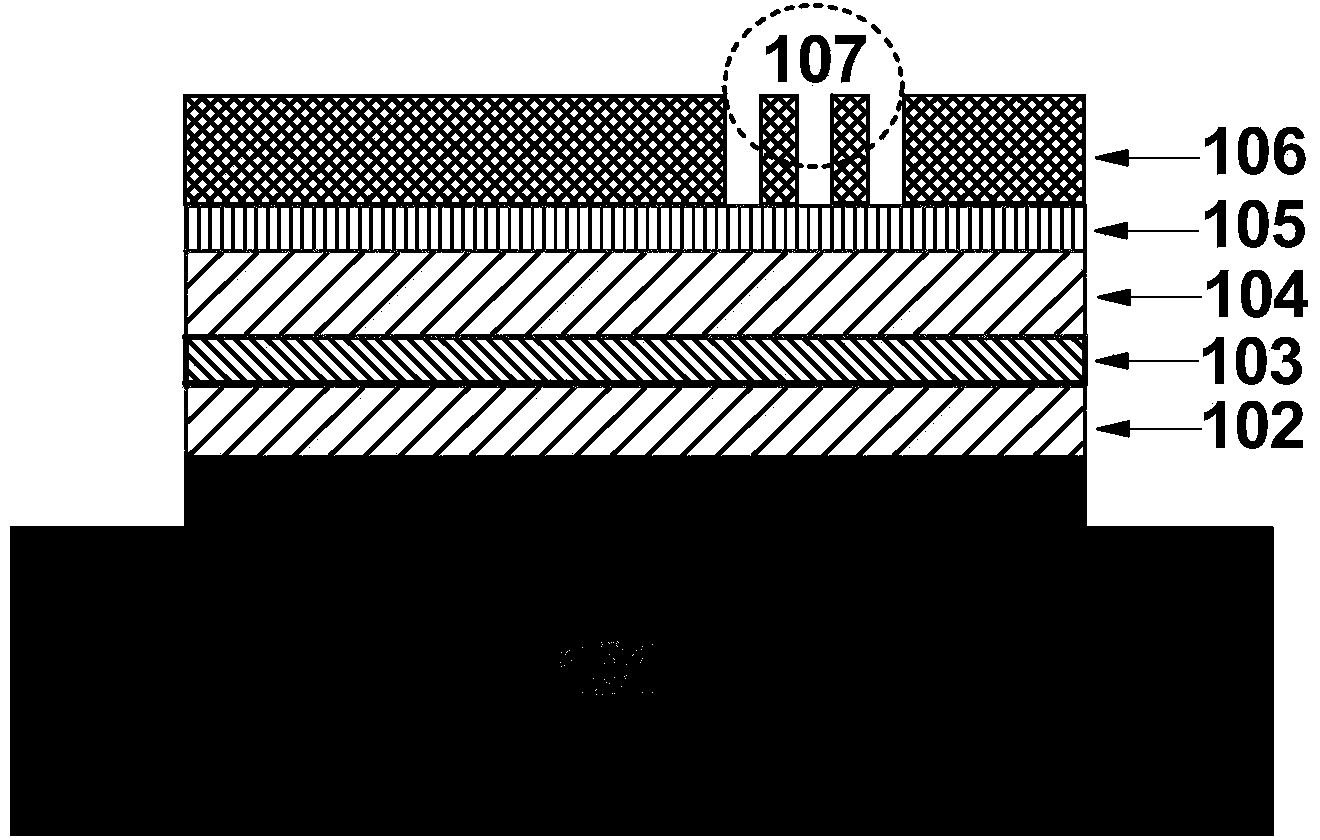
[0042] figure 1 It is a schematic diagram of the structure of the surface plasmon electric excitation source. A surface plasmon electric excitation source with a dielectric-metal near-field coupling structure, including a substrate 101, a semiconductor quantum well epitaxial layer, a metal layer 106, and a coupling output structure 107; the semiconductor quantum well epitaxial layer is loaded on The surface of the substrate 101 ; the metal layer 106 is carried on the surface of the semiconductor quantum well epitaxial layer, and the outcoupling structure 107 is located in the metal layer 106 .

[0043] The semiconductor quantum well epitaxial layer includes a quantum well structure layer and a p-type ohmic contact layer 105; ...

Embodiment 2

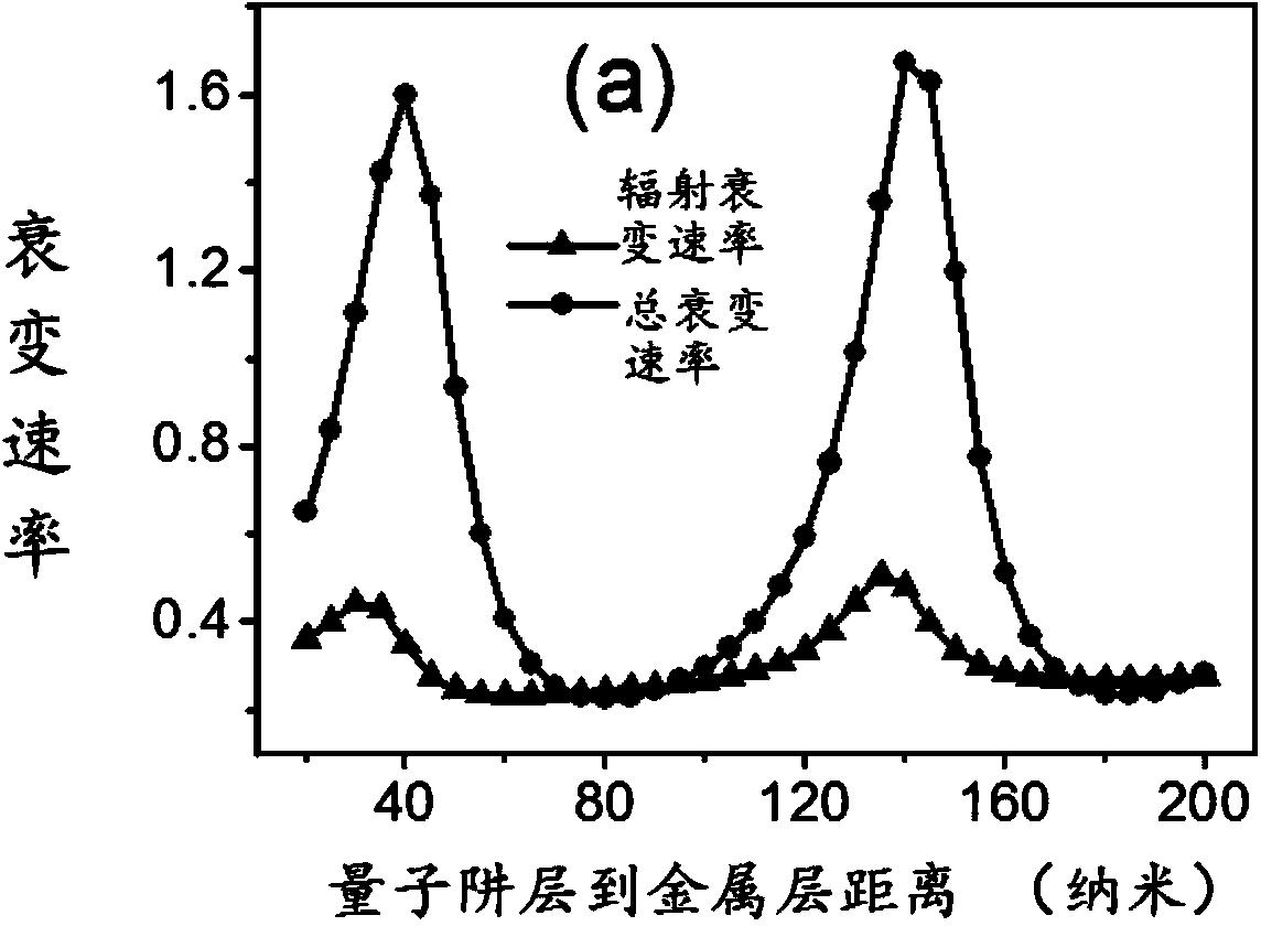
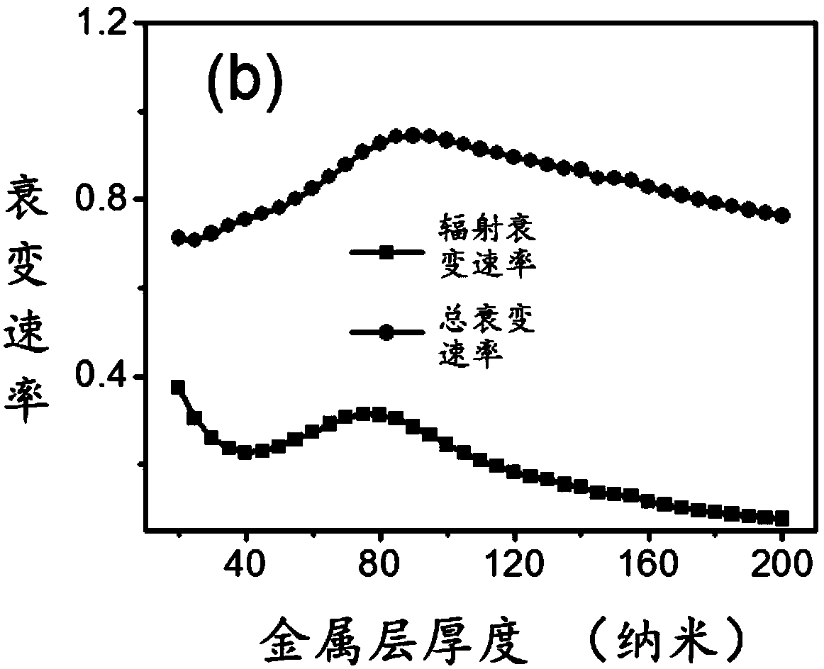
[0052] A surface plasmon electric excitation source with a dielectric-metal near-field coupling structure and its manufacturing method, repeating Example 1, the difference is that the semiconductor quantum well epitaxial layer has a wavelength range of 0.9-1.6 μm InP-based material; due to the increased working wavelength, the optimal distance between the quantum well layer 103 and the metal layer 106 is about 40-60nm, and the thickness of the metal layer 106 is about 90-120nm. The coupling output structure is a hole array.

Embodiment 3

[0054] A surface plasmon electric excitation source with a dielectric-metal near-field coupling structure and its manufacturing method, repeating Example 1, the difference is that the semiconductor quantum well epitaxial layer has a wavelength range of 0.4-0.6 μm GaN-based material; due to the short working wavelength, the optimum distance between the quantum well layer 103 and the metal layer 106 is about 25-35nm, and the thickness of the metal layer 106 is about 60-90nm. The coupling output structure is a grating structure.

[0055] In the preparation method of a surface plasmon electric excitation source with a dielectric-metal near-field coupling structure described in the present invention, firstly, electron beam exposure or photolithography is used to obtain the pattern of the coupling output structure on the quantum well epitaxial layer , and then deposit metal, and then use the method of stripping with glue, and the device can also be realized. However, the quantum we...


PUM


Abstract

The invention discloses a surface plasmon excimer electrically-induced excitation source with a medium-metal near field coupling structure. The surface plasmon excimer electrically-induced excitation source comprises a substrate, semiconductor quantum well epitaxial layer, a metal layer and a coupling output structure. The semiconductor quantum well epitaxial layer is loaded on the surface of the substrate. The metal layer is loaded on the surface of the semiconductor quantum well epitaxial layer. The coupling output structure is located in the metal layer. The invention further discloses a manufacturing method of the surface plasmon excimer electrically-induced excitation source. The method includes the steps that the semiconductor quantum well epitaxial layer is grown on the substrate; a device unit is etched on the grown semiconductor quantum well epitaxial layer; the metal layer is deposited on the etched device unit; the coupling output structure is manufactured in the deposited metal layer. According to the surface plasmon excimer electrically-induced excitation source, the semiconductor quantum well material is adopted to serve as an active medium, based on the near field coupling principle, the quantum efficiency is high, the light emitting wavelength range is wide, the excitation efficiency is high, the manufacturing process is simple, integration is conducted conveniently, and the surface plasmon excimer electrically-induced excitation source and the manufacturing method have great research value and application prospects.

Description

technical field [0001] The invention relates to a surface plasmon device and a manufacturing method thereof. More specifically, it relates to a surface plasmon electric excitation source with a dielectric-metal near-field coupling structure and a manufacturing method thereof. Background technique [0002] As the operating frequency and integration of microelectronic integrated circuits are increasingly approaching the physical limit, using only electrons as information carriers can no longer meet the requirements of high-speed, large-capacity transmission and processing. Compared with electronic circuits, photonic integrated circuits that use photons to carry information have the advantages of high frequency, low loss, and high transmission bandwidth. Transmission and control of light at the nanoscale. Surface plasmon polaritons (Surface Plasmon Polariton, SPP) are faster than electrons and can break through the diffraction limit. Therefore, plasmonic integrated circuits ...

Claims


Application Information

Patent Timeline
Patent Type & Authority Applications(China)
IPC IPC(8): H01L33/00H01L33/06H01L33/14
CPCH01L33/005H01L33/06H01L33/14H01L2933/0008
Inventor 李敬孟祥敏
Owner TECHNICAL INST OF PHYSICS & CHEMISTRY - CHINESE ACAD OF SCI
Why Eureka
Try Eureka