Inverted packaging technology for wafer-level LED

A light-emitting diode, flip-chip packaging technology, applied in the direction of electrical components, circuits, semiconductor devices, etc., can solve the problems of inconsistent thickness of phosphor glue, inconsistent chip light color, long time, etc., to achieve the consistency of color and color temperature Good, uniform coating thickness, high process efficiency

Inactive Publication Date: 2012-07-18
连云港陆亿建材有限公司 +1
View PDF5 Cites 15 Cited by
  • Summary
  • Abstract
  • Description
  • Claims
  • Application Information

AI Technical Summary

Problems solved by technology

The method of needle drop coating is not a very repeatable process, and it is easy to cause inconsistent thickness of phosphor glue and inconsistent col...

Method used


Image

  • Inverted packaging technology for wafer-level LED
  • Inverted packaging technology for wafer-level LED
  • Inverted packaging technology for wafer-level LED

Examples


Embodiment 1

[0024] Such as figure 2 As shown, the wafer-level light-emitting diode flip-chip packaging process in the embodiment of the present invention includes the following steps:

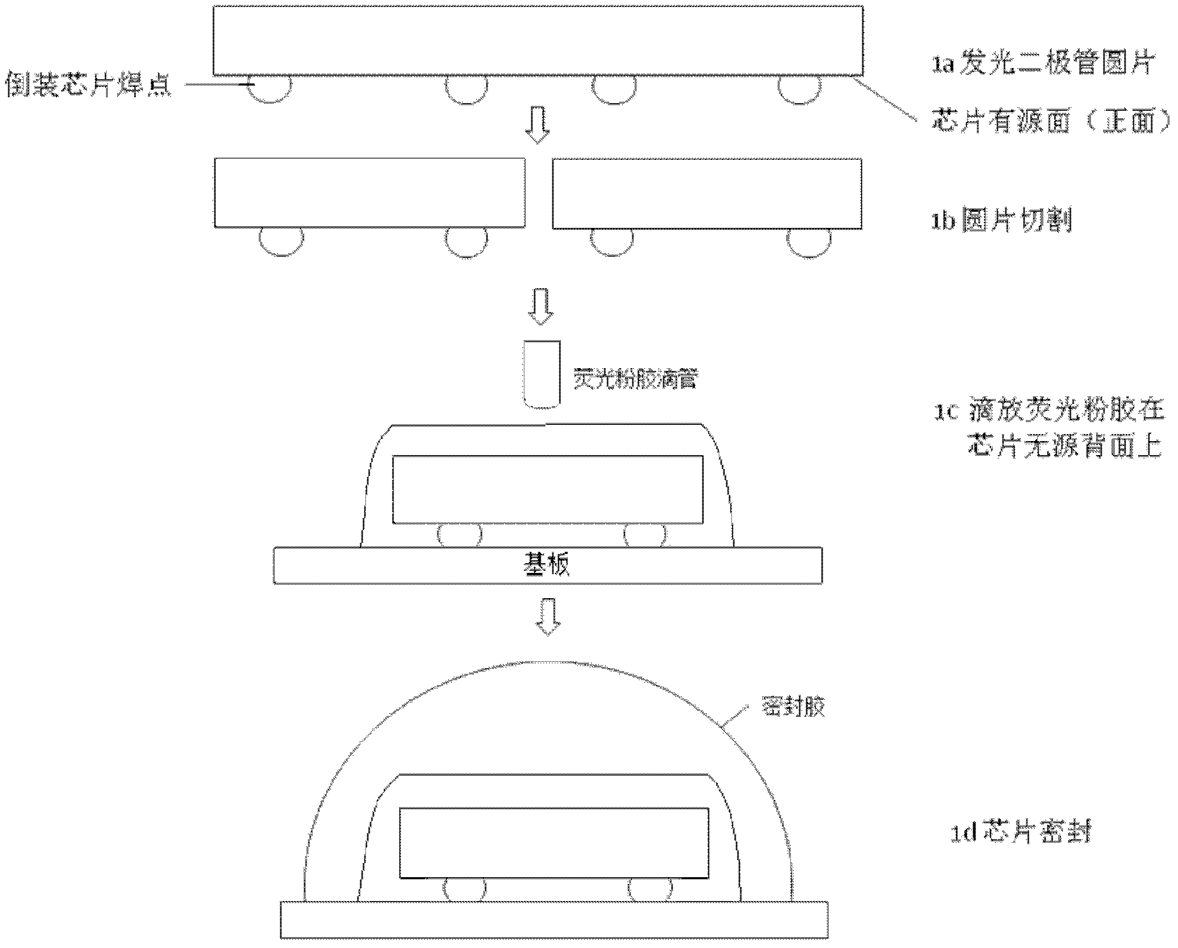
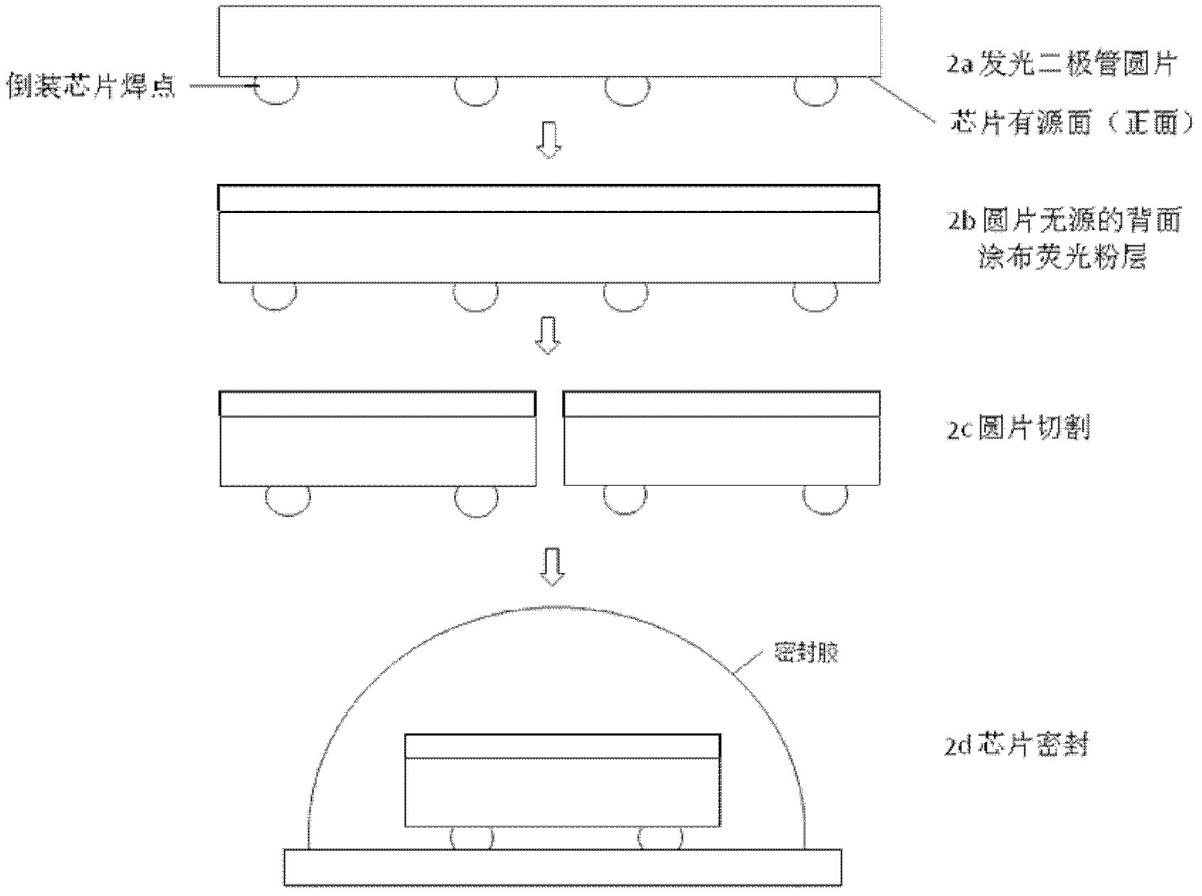
[0025] 4a——Make chip soldering points on the front side of the LED wafer.

[0026] 4b——Coating phosphor glue on the back of the light-emitting diode wafer and curing it, so that a layer of thick and uniform phosphor coating is formed on the back of the light-emitting diode wafer.

[0027] The coating methods of phosphor glue include spin coating, spray coating, lamination and other methods. Typically during the spin coating process, the wafer is vacuumed onto a rotary table. There are many electrode bumps (chip soldering points) on the flip-chip wafer, which cannot be vacuum-adsorbed onto the rotary table. Therefore, the wafer can be placed face down on a flat plate with a thin layer of high adhesive, and the flat plate is vacuum adsorbed on the rotary table. Another method is to use an uncured thick ...

Embodiment 2

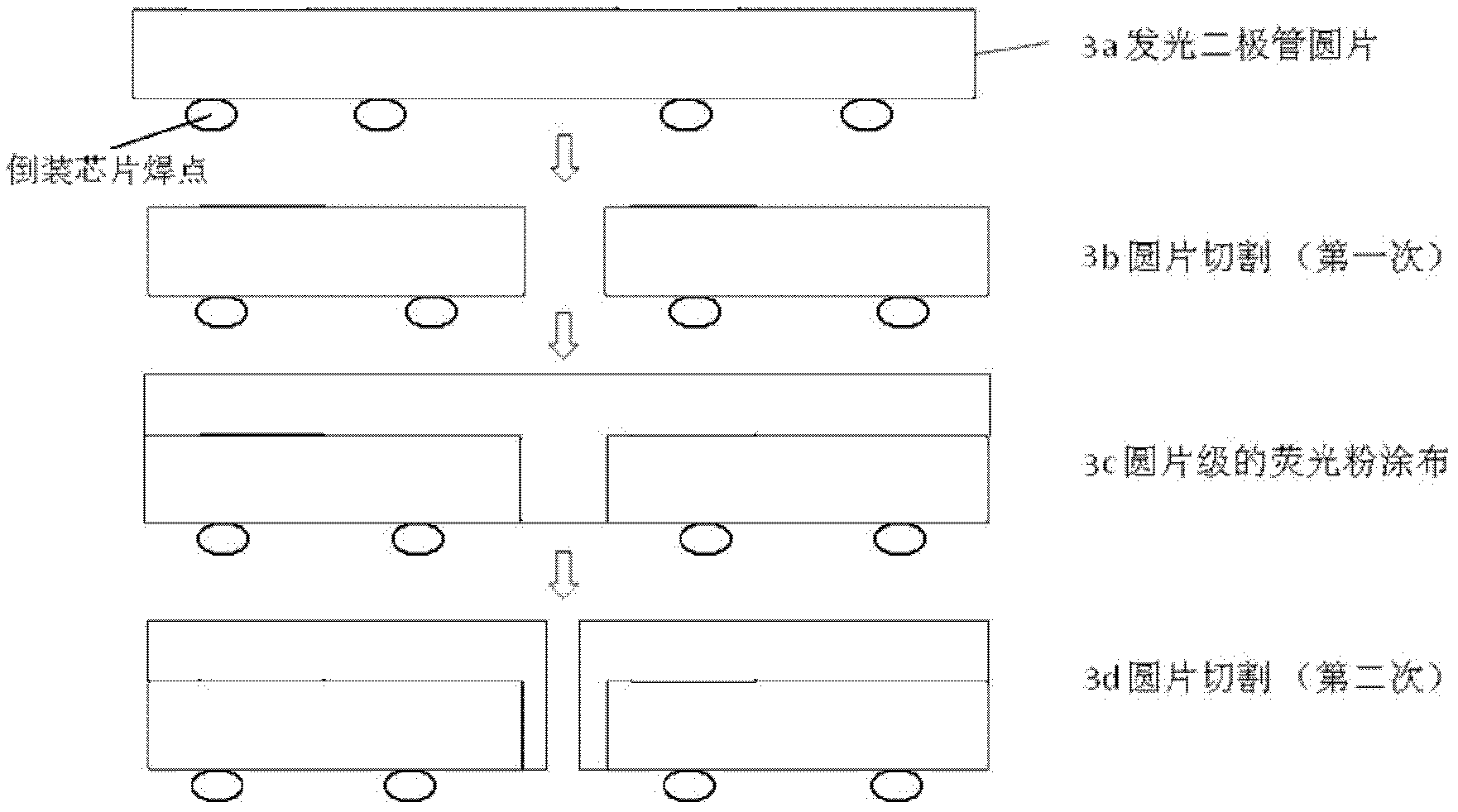
[0033] In order to make the side of the chip emit light, in this embodiment, a phosphor coating is also coated on the side of the light-emitting diode wafer. The proportion of light emitted from the side of the chip depends on the type and size of the chip. For a vertical chip of about 1 mm, there is about 15% side light. For a horizontal chip of the same size, the side light is about 30%. For chips a few millimeters in size, the side light may be reduced to less than 10% of the total luminous flux.

[0034] The realization method of this structure is the improvement on the basis of embodiment 1 technique. Such as image 3 shown, including the following steps:

[0035] 5a——Make chip soldering points on the front side of the light-emitting diode wafer;

[0036] 5b——cutting the light-emitting diode wafer (using a wider grinding wheel or laser beam cutting);

[0037] 5c——While coating phosphor glue on the back of the light-emitting diode wafer, the gap between the light-emi...


PUM


Abstract

The invention discloses an inverted packaging technology for a wafer-level LED. The technology comprises the following steps: fluorescent powder glue is coated on the back side of an LED wafer; the wafer with a fluorescent powder coating is divided into individual chips; the LED chips with front side facing downwards are arranged on a baseplate; and the chips and the baseplate are welded and fixed through chip soldering points and are sealed by glue through irrigation. The packaging technology provided by the invention has the advantages that the wafer-level fluorescent powder coating is uniform in thickness, so that the wavelength distribution and color of light given out by the different chips are ensured to be consistent; and besides, the fluorescent powder glue can be coated on the LED wafer at one time, the coating technology for individual chips is avoided, and the production efficiency is improved.

Description

technical field [0001] The invention relates to a wafer-level light-emitting diode flip-chip packaging process. Background technique [0002] Coating a phosphor powder coating on a light-emitting diode chip is one of the main methods to change the wavelength and color of the light emitted by the chip. For example, the commonly used white light lighting scheme of LEDs is to coat phosphor glue that excites yellow light on the blue LED chip, and the blue light emitted by the chip and part of the yellow light excited by the phosphors are synthesized to form white light. The problem with the current phosphor coating on the surface of the chip is that the thickness of the coating produced by the traditional colloid dispensing process is not uniform, and the coating process efficiency of a single chip is low. Another problem with flip-chip is that the phosphor glue that is dispensed will flow from the side of the chip to the substrate, and will further flow into the gap between th...

Claims


Application Information

Patent Timeline
IPC IPC(8): H01L33/50H01L33/56
Inventor 宋永江陈荣高赵一凡陆振刚卢基存
Owner 连云港陆亿建材有限公司
Why Eureka
Try Eureka