cmos operational amplifier with very large dc open-loop voltage gain
A technology of operational amplifier and voltage gain, applied in DC-coupled DC amplifiers, differential amplifiers, etc., can solve the problems of limited improvement and achieve the effects of wide unity gain bandwidth, multiple power consumption, and short settling time
- Summary
- Abstract
- Description
- Claims
- Application Information
AI Technical Summary
Problems solved by technology
Method used
Image
Examples
Embodiment Construction
[0031] In order to make the technical problems, technical solutions and advantages to be solved by the present invention clearer, the following will describe in detail with reference to the drawings and specific embodiments.
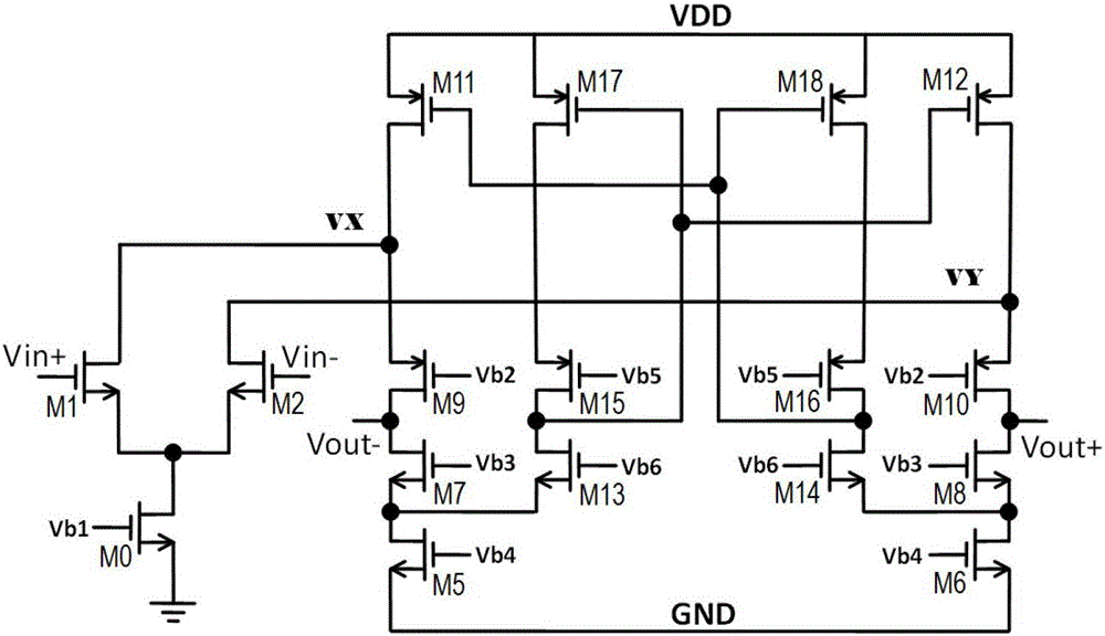
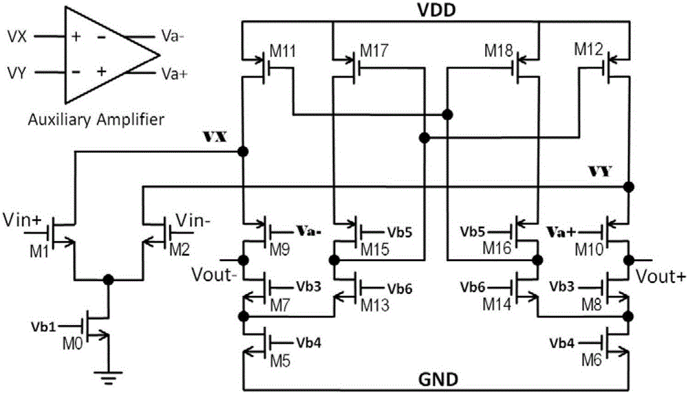
[0032] like figure 1 As shown, it is a circuit diagram of an operational amplifier of an embodiment of the present invention. In this circuit, nodes Vin+ and Vin- are respectively the positive and negative input terminals of the operational amplifier, and nodes Vout+ and Vout- are respectively the positive and negative input terminals of the operational amplifier. The output terminal and the negative output terminal, the node VDD and the node GND are respectively connected to the power supply voltage and the ground voltage. The operational amplifier of this embodiment includes: a first transistor M0, a second transistor M1, a third transistor M2, a fifth transistor M5, a sixth transistor M6, a seventh transistor M7, an eighth transistor M8, a ninth trans...
PUM
 Abstract
Description
Claims
Application Information


