
Gate drive circuit, array substrate and display device

A gate drive circuit and array substrate technology, applied in the field of array substrates, display devices, and gate drive circuits, can solve the problems of short data signal writing time, abnormal screen display, and inability to meet user display effect requirements, etc. The effect of increasing write time and reducing likelihood

Active Publication Date: 2014-08-13
HEFEI BOE OPTOELECTRONICS TECH +1
View PDF5 Cites 16 Cited by
  • Summary
  • Abstract
  • Description
  • Claims
  • Application Information

AI Technical Summary

Problems solved by technology

[0005] However, since the resolution of the current liquid crystal display is getting higher and higher, the writing time of the data signal when the gate line signal is output is getting shorter and shorter.
If the gate line drive circuit in the prior art is also used, it is easy to cause abnormal display of the picture due to insufficient writing time of the data signal, so that the high-resolution liquid crystal display is prone to display failure, which cannot meet the user's requirements for display effect. Require

Method used


Image

  • Gate drive circuit, array substrate and display device
  • Gate drive circuit, array substrate and display device
  • Gate drive circuit, array substrate and display device

Examples


Embodiment Construction

[0038] In order to make the purpose, technical solutions and advantages of the embodiments of the present invention clearer, the technical solutions in the embodiments of the present invention will be clearly and completely described below in conjunction with the drawings in the embodiments of the present invention. Obviously, the described embodiments It is a part of embodiments of the present invention, but not all embodiments. Based on the embodiments of the present invention, all other embodiments obtained by persons of ordinary skill in the art without creative efforts fall within the protection scope of the present invention.

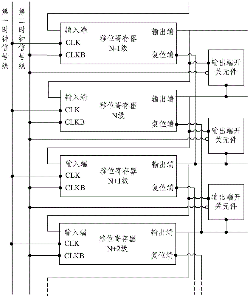
[0039] An embodiment of the present invention proposes a gate drive circuit, see figure 1 , the gate drive circuit includes a multi-stage shift register, and each stage of the shift register is connected to the first clock signal line and the second clock signal line.

[0040] Wherein, for any integer N not less than 2, the input end of the Nth s...


PUM


Abstract

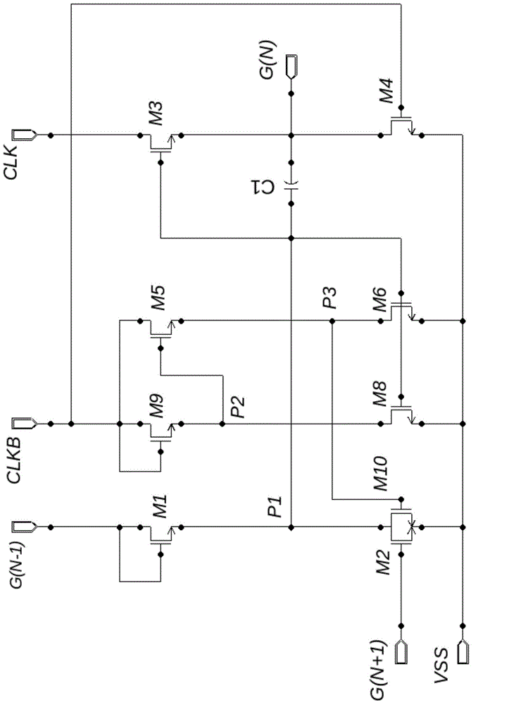
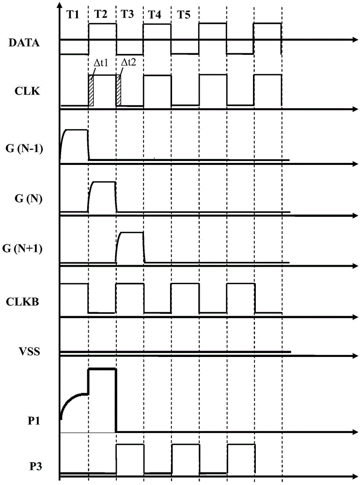
The invention relates to the field of display technologies, in particular to a gate drive circuit, an array substrate and a display device. Based on the prior art, an output end switching element controlled by second clock signals is additionally arranged between the input end and the output end of a shifting register in each level, and the original reset connection mode between the output end of the next level and the reset end of the upper level is changed to be the reset connection mode between the output end of the N+2 level and the reset end of the N level. Under the design, gate line output signals of the shifting register in each level in the gate drive circuit can be output in advance, the continuous output time of the gate line output signals is doubled, so that write time of data signals is greatly increased, and occurring possibility of display failures is reduced.

Description

technical field [0001] The present invention relates to the field of display technology, in particular to a gate drive circuit, an array substrate and a display device. Background technique [0002] Thin film transistor liquid crystal display (TFT-LCD for short) is one of most liquid crystal display screens, which adopts thin film transistor technology, which can significantly improve image quality. [0003] As an important part of the TFT-LCD driver, the main function of the gate drive circuit is to convert the input clock signal through the shift register and add it to the gate line of the liquid crystal display panel. In the multi-stage shift register of the gate driving circuit, each stage is connected to a corresponding gate line to output a gate line driving signal. In the gate drive circuit, the shift registers at all levels are connected to each other, the start signal is input to the first level of each level, and the gate line drive signals are output to the gate ...

Claims


Application Information

Patent Timeline
Patent Type & Authority Applications(China)
IPC IPC(8): G09G3/36G09G3/20
CPCG09G3/3677G09G2310/0286G09G2300/0408G11C19/28G09G3/36G09G3/20
Inventor 张晓洁邵贤杰李小和薛伟董职福
Owner HEFEI BOE OPTOELECTRONICS TECH
Learn More