Display device, a driving method of a display device, and a semiconductor integrated circuit incorporated in a display device

a display device and driving method technology, applied in the field of display devices, can solve the problems of low display quality in the display device, and achieve the effect of driving more accurately and suppressing power consumption

Inactive Publication Date: 2011-06-14
SEMICON ENERGY LAB CO LTD
View PDF60 Cites 2 Cited by
  • Summary
  • Abstract
  • Description
  • Claims
  • Application Information

AI Technical Summary

Benefits of technology

[0020]Moreover, in the case of the voltage input method adopting the analog gray scale method, a display device is easily affected by variations in TFTs as described above. On the other hand, in the case of the current input method, the writing time of a signal current is lengthened.
[0053]According to the invention, a signal current supplied to a light emitting element can be corrected as the light emitting element varies with time, whereby reducing display variations due to image persistence. Also according to the invention, luminance decay of a light emitting element due to the degradation thereof can be prevented by setting a signal current corresponding to the degradation of the light emitting element, leading to the prevention of lowered image quality.
[0055]Further, according to the invention, a signal current corrected in accordance with the degradation of each light emitting element can be set. Therefore, each light emitting element can be driven more accurately as compared with in the case of correcting a signal current depending on the most degraded light emitting element, and power consumption can be suppressed.

Problems solved by technology

The image persistence causes low quality display in the display device.

Method used


Image

  • Display device, a driving method of a display device, and a semiconductor integrated circuit incorporated in a display device
  • Display device, a driving method of a display device, and a semiconductor integrated circuit incorporated in a display device
  • Display device, a driving method of a display device, and a semiconductor integrated circuit incorporated in a display device

Examples


embodiment mode 1

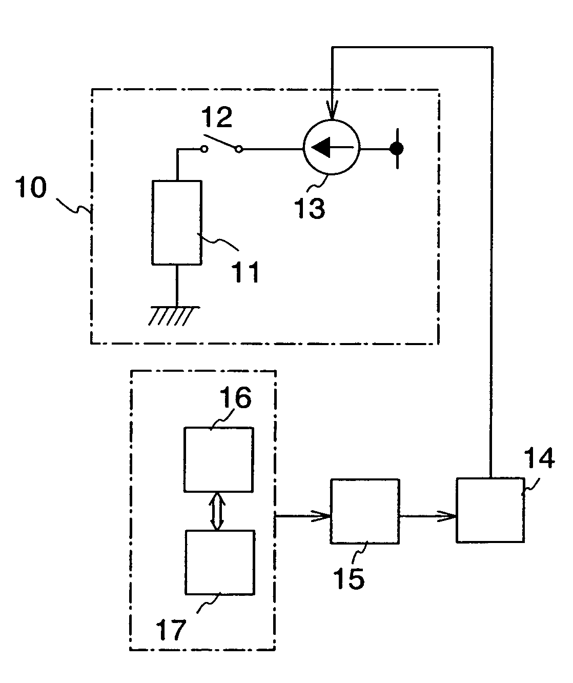
[0076]In this embodiment mode, a function and a configuration of a display device of the invention is described.

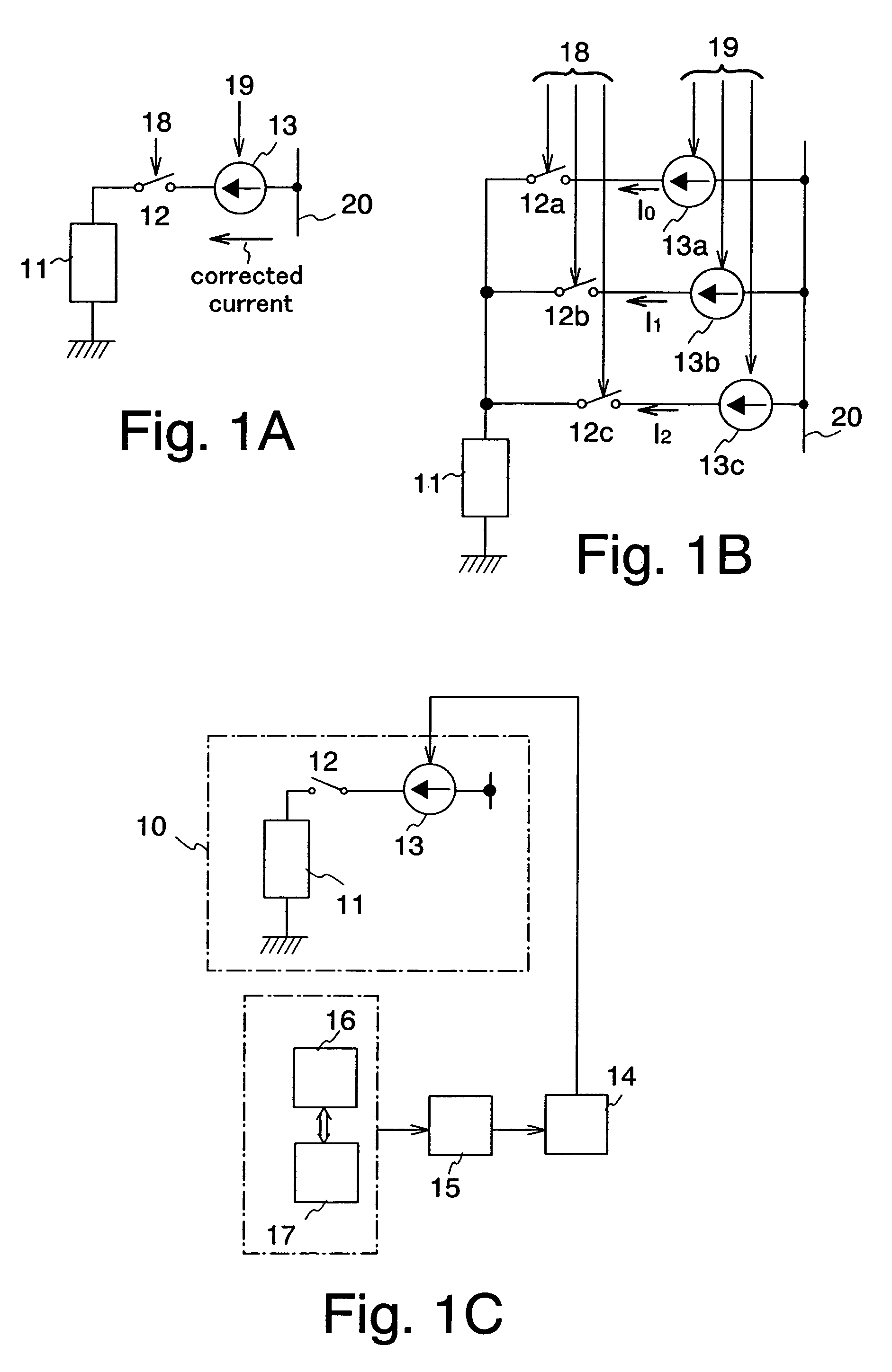
[0077]As shown in FIG. 1A, a display device of the invention, particularly a pixel thereof comprises a light emitting element 11 and a current source 13 (hereinafter referred to as a driving current source) connected to the light emitting element 11 via a switch 12. The switch 12 has a function of switching a light emission and a non-light emission by selecting according to a video signal 18 whether a current from the current source 13 is supplied to the light emitting element 11 or not. The driving current source 13 is connected to a power supply line 20 and controlled by a signal 19 (hereinafter referred to as a control signal) which is different from the video signal 18. It is to be noted that components other than the switch 12 may be provided between the light emitting element 11 and the driving current source 13. In other words, it is only necessary that the light em...

embodiment mode 2

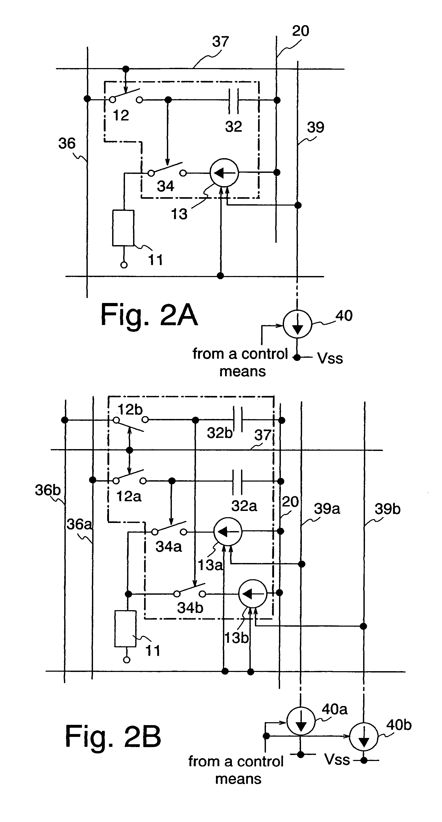
[0096]In this embodiment mode, a specific pixel configuration of the invention is described with reference to FIGS. 2A and 2B.

[0097]As shown in FIG. 2A, a pixel comprises at least the light emitting element 11 and an area surrounded by a dotted line which includes a switch 12, the driving current source 13, a capacitor 32, and a switch 34 provided between the driving current source 13 and the light emitting element 11. The switch 12 is connected to a signal line 36 and a scan line 37, and the driving current source 13 and the capacitor 32 are connected to a power supply line 20. A signal from a signal supply current source 40 is input to the driving current source 13 via a current line 39. As described above, the signal supply current source 40 is controlled by a control means and a signal for controlling the switch of the driving current source 13 is input to the signal supply current source 40.

[0098]Moreover, a plurality of driving current sources 13a and 13b may be provided as sh...

embodiment mode 3

[0115]Many methods are possible to correct a signal current in accordance with the degradation of a light emitting element. That is, the invention is characterized in that a current value is corrected depending on the degradation of a light emitting element, and the method of correcting the current value and the like is not exclusively limited.

[0116]In this embodiment mode, shown is a method of correcting a signal current supplied to a light emitting element by using two current sources. Note that in this invention, a single or a plurality of current sources may be employed for correcting a signal current.

[0117]In FIG. 12A, a first current source 21 and a second current source 22 for setting a corrected signal current are shown. The first current source 21 and the second current source 22 are used as a reference current source and a correction current source respectively. The first and the second current sources 21 and 22 are connected to the same current line, and also connected to...


PUM


Abstract

A display device in which a current supplied to a light emitting element is corrected depending on a degradation level of the light emitting element and display variations due to the degradation of each light emitting element are suppressed. Further, according to the display device of the invention, the effect of variations in TFTs is reduced and writing time of a signal is shortened. To achieve the aforementioned display device, according to the invention, a current value supplied to a light emitting element is corrected in accordance with the degradation thereof instead of correcting a video signal. Further, the display device comprises at least a supply source for supplying a corrected current depending on the degradation of a light emitting element and a current source for supplying the corrected current from the supply source to the light emitting element. Moreover, according to such a display device, a first current source of the supply source supplies a corrected current corresponding to the degradation of the least degraded light emitting element of the light emitting elements connected to the same signal line, meanwhile a second current source supplies a corrected current corresponding to the degradation of the most degraded light emitting element of the light emitting elements connected to the same signal line.

Description

BACKGROUND OF THE INVENTION[0001]1. Field of the Invention[0002]The present invention relates to a display device, particularly an active matrix display device having self-light emitting elements, and to a driving method of a display device. The invention further relates to a semiconductor integrated circuit incorporated in a display device.[0003]2. Description of the Related Art[0004]In recent years, a display device using a light emitting element (self-light emitting element) has been studied and developed. Such a display device has the advantages of high image quality, reduced thickness, light weight or the like, and thus it is widely used as a screen of a mobile phone and a monitor of a personal computer. In particular, since the light emitting display device has the features such as low voltage drive, low power consumption, and fast response which contributes to dynamic display, it is expected to be used for various electronic apparatuses typified by a next-generation mobile ph...

Claims


Application Information

Patent Timeline
Patent Type & Authority Patents(United States)
IPC IPC(8): G09G3/32G09F9/30G09G3/20G09G3/30H05B33/14H05B44/00
CPCG09G3/3291G09G3/3233G09G2300/0819G09G2300/0842G09G2320/048G09G2300/0861G09G2320/0252G09G2320/043G09G2300/0852
Inventor KIMURA, HAJIMEKOYAMA, JUN
Owner SEMICON ENERGY LAB CO LTD
Why Eureka
Try Eureka