Memory write timing system

a memory write and timing system technology, applied in the field of memory write timing system, can solve the problems of difficulty in writing memory array bitcells, time-consuming, and dramatically affecting the performance of integrated circuits, and achieve the effect of simplifying the scaling of delays

Active Publication Date: 2008-04-10
ANALOG DEVICES INC
View PDF8 Cites 1 Cited by
  • Summary
  • Abstract
  • Description
  • Claims
  • Application Information

AI Technical Summary

Benefits of technology

[0006]It is a further object of this invention to provide such an improved memory write timing system which will not complete the write cycle before a standard write would, yet will not long delay completion of the write cycle thereafter.
[0007]It is a further object of this invention to provide such an improved memory write timing system which properly times a write operation even in extreme comer conditions of low voltage, low temperature and skewed processing e.g. slow NFET and fast PFET operation.
[0008]It is a further object of this invention to provide such an improved memory write timing system which even in comer conditions tracks the more complex changes in timing operation of bitcells beyond the simpler scaling of delays that occur in most logic paths.
[0009]The invention results from the realization that an improved memory write timing system which closely tracks standard bitcell operation across process and environmental variables, can be achieved with a modified memory bitcell including a modified memory bitcell including a storage device and a write / read circuit for writing / reading data to / from the storage device; and an output circuit for detecting the current state of the storage device and more particularly in the case of an SRAM a modified memory bitcell including a pair of inverters in a latching configuration having first and second nodes with an access device connected to at least one node and an output circuit connected to one of the nodes for indicating the state of the modified bitcell and providing a write termination signal.

Problems solved by technology

Device performance in integrated circuits can be dramatically affected by extreme comers: extremes in temperature, operating voltage, and wafer processing.
For certain combinations of these extreme comers, degraded device performance can cause difficulty writing the bitcells of memory arrays .e.g.
However, building into control circuitry a longer amount of time to perform writes can also limit the performance of the memory at other comers.
For instance, in this type of scenario the timing column may slow down by a factor of five while the bitcells may slow down by a factor of ten, causing the write to fail.
Since bitcells don't respond to process variations in the same way as the timing chain or delay circuits at extreme corners, the introduced delay is not sufficient and the operation terminates before the write actually occurs.
First, since the read operation is normally longer than the write operation, time is wasted in the write operation.
Second, in extreme comer conditions, the write can be slower than the read and the write operation is cut off before the write is complete.

Method used


Image

  • Memory write timing system
  • Memory write timing system
  • Memory write timing system

Examples


Embodiment Construction

[0022]Aside from the preferred embodiment or embodiments disclosed below, this invention is capable of other embodiments and of being practiced or being carried out in various ways. Thus, it is to be understood that the invention is not limited in its application to the details of construction and the arrangements of components set forth in the following description or illustrated in the drawings.

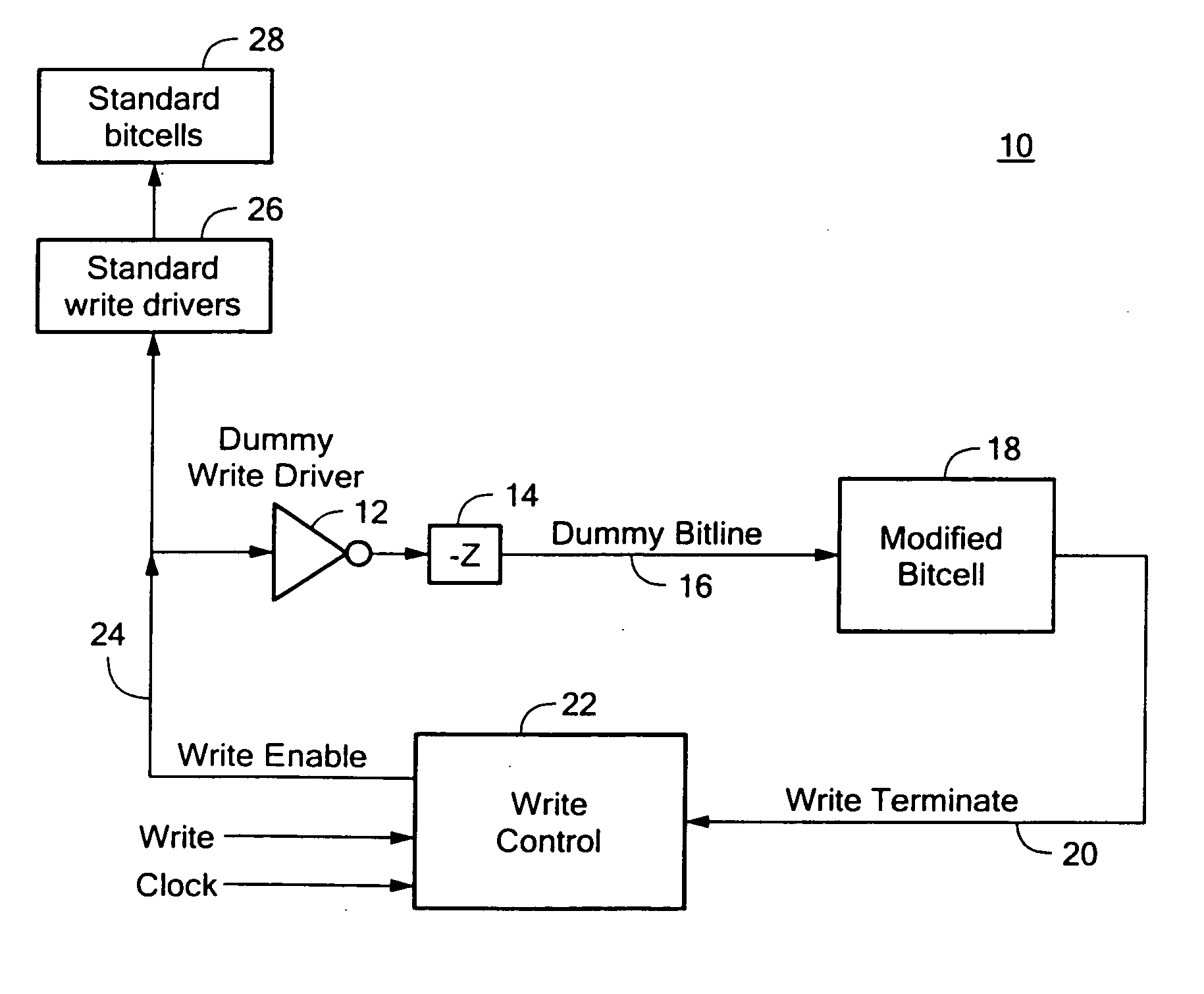
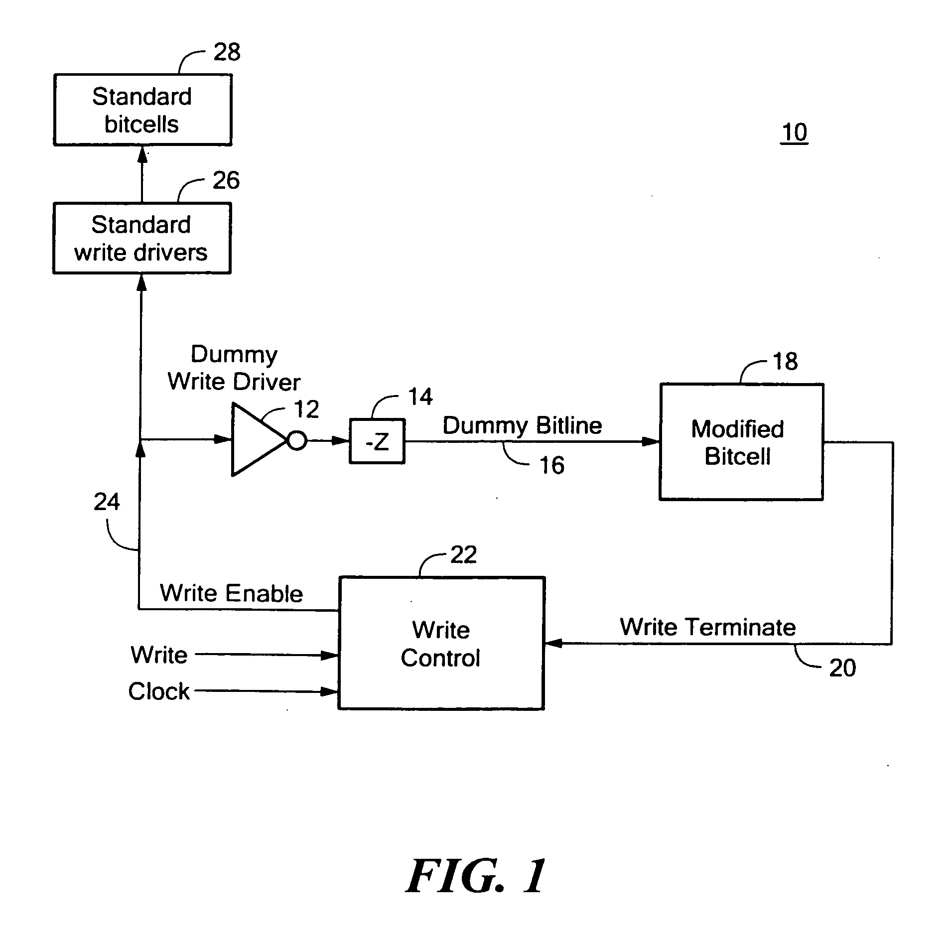
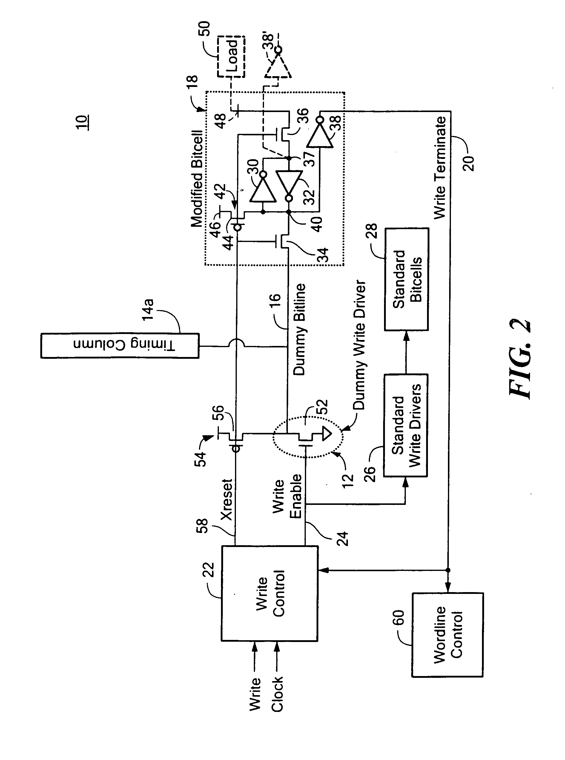
[0023]There is shown in FIG. 1 a memory write timing system 10, according to this invention, which includes a dummy write driver 12, a delay 14 representing a delay introduced by a normal bit line, and a dummy bit line 16 which connects dummy write driver through delay 14 to a modified bitcell 18. Bitcell 18 is modified because in addition to a storage device there is at least an output circuit connected to a node of the bitcell for indicating a state of the bitcell and providing a write termination signal on line 20 to write control 22.

[0024]In operation upon receiving a write command and ...


PUM


Abstract

A memory write timing system includes a modified memory bitcell including a storage device and a write/read circuit for writing/reading data to/from the storage device; and an output circuit for detecting the current state of the storage device.

Description

FIELD OF THE INVENTION[0001]This invention relates to an improved memory write timing system and more particularly to such a system which tracks standard memory bitcell operation time across process and environmental variables.BACKGROUND OF THE INVENTION[0002]Device performance in integrated circuits can be dramatically affected by extreme comers: extremes in temperature, operating voltage, and wafer processing. For certain combinations of these extreme comers, degraded device performance can cause difficulty writing the bitcells of memory arrays .e.g. SRAM's, DRAM's. For at least some of these extreme comers, bitcell writing can still be successfully achieved if sufficient time is allowed for that operation. However, building into control circuitry a longer amount of time to perform writes can also limit the performance of the memory at other comers.[0003]In mobile applications, for example, the operating voltage may be decreased during periods of inactivity to save battery power. ...

Claims


Application Information

Patent Timeline
Patent Type & Authority Applications(United States)
IPC IPC(8): G11C11/00G11C7/00
CPCG11C7/02G11C7/04G11C7/1078G11C7/1096G11C7/14G11C7/22G11C29/50012G11C11/4096G11C11/41G11C29/028G11C29/24G11C29/50G11C11/4076
Inventor HOLLIS, PAUL W.LATTIMORE, GEORGE M.
Owner ANALOG DEVICES INC
Why Eureka
Try Eureka