Matrix substrate and display which inputs signal-polarity inverting signals to picture data

a matrix substrate and picture data technology, applied in the field of matrix substrates, can solve the problems of high electric properties of display apparatuses, high cost of display equipment, and rapid increase of manufacturing costs, so as to reduce the load of one d/a converter, reduce the number and kinds of constituting parts, and reduce the load of picture signal lines

Inactive Publication Date: 2014-07-01
CANON KK
View PDF37 Cites 3 Cited by
  • Summary
  • Abstract
  • Description
  • Claims
  • Application Information

AI Technical Summary

Benefits of technology

[0018]In the liquid crystal device of the present invention, the number and kinds of the constituting parts can be reduced in the external driving circuit, and the load to the picture signal lines can be reduced by employing digital input instead of analog input in conventional liquid crystal device. Further, the load to one D / A converter can be reduced and the time of writing into the liquid crystal picture element can be lengthened. Thereby, the entire power consumption of the liquid crystal can be reduced, the picture can be made finer, adverse influence of noises can be reduced, and picture quality can be improved.

Problems solved by technology

However, with the increase of the picture size, the display manufacture equipment becomes expensive, and display apparatus requires high levels of the electric properties for driving the larger picture display.
With the increase of the picture size, the manufacture cost increases rapidly in proportion to 2-3th power of the picture size.
Therefore, the transfer switch is required to conduct the transfer at an extremely high rate, which necessitates a larger size of the transfer switch.
Furthermore, the wiring is necessary for connecting the above common signal lines to pads for connection to an external circuit, which results in a large capacitance of the common signal lines.
In the liquid crystal display element, the amplitude of the analog picture signals is as high as 10 V or more, which requires a high performance of the external driving circuit for driving the load of high capacitance at a large amplitude at a high speed, and requires a high power consumption, disadvantageously.
Therefore, the length of the cable is limited which reduces mechanical freedom disadvantageously.
This is not practical.

Method used


Image

  • Matrix substrate and display which inputs signal-polarity inverting signals to picture data
  • Matrix substrate and display which inputs signal-polarity inverting signals to picture data
  • Matrix substrate and display which inputs signal-polarity inverting signals to picture data

Examples


first embodiment

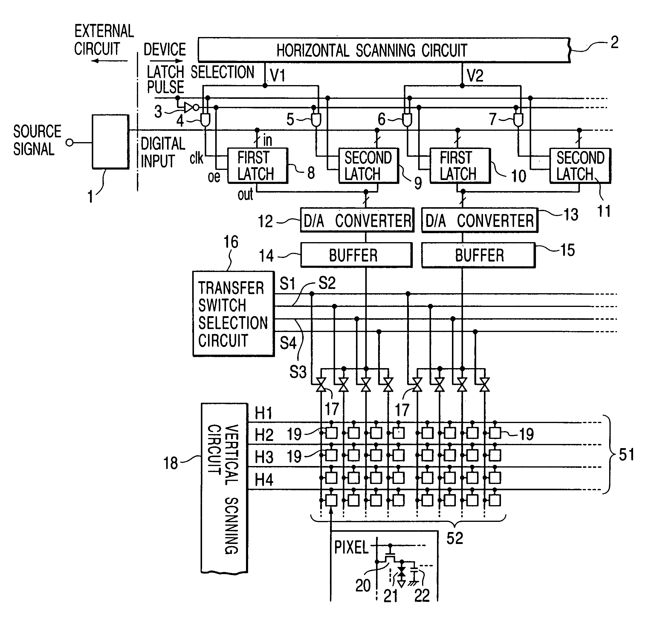
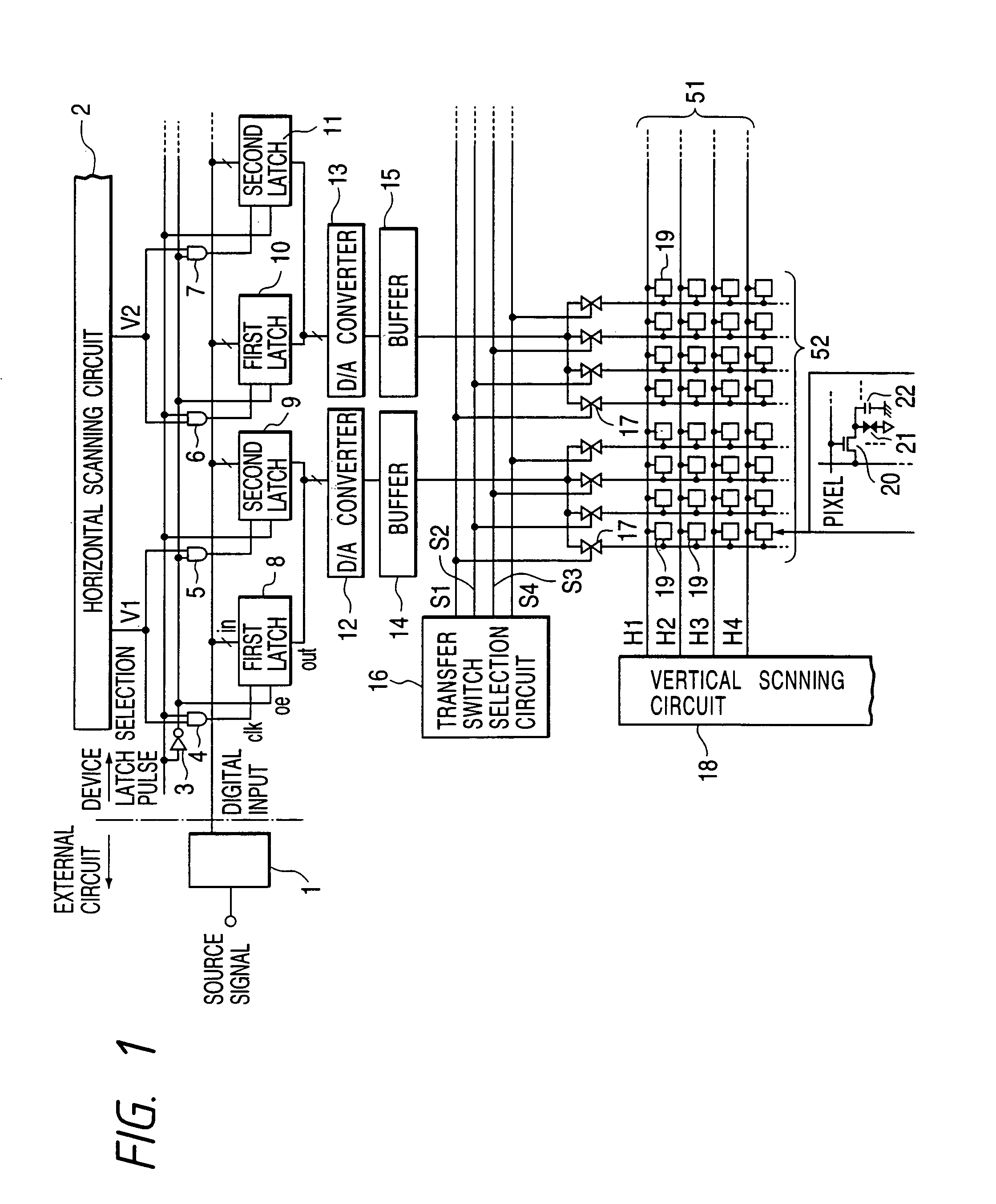
[0060]FIG. 1 is an equivalent circuit diagram showing a first embodiment of the present invention. The device of this embodiment comprises plural vertical signal lines for the output from a horizontal scanning circuit, plural scanning lines for the output from vertical scanning circuit (shift register) 18, and picture element electrodes formed at the intersecting points of the vertical signal lines and the scanning lines with interposition of switches. Scanning lines 51 (H1-H4 . . . ) are connected to vertical scanning circuit 18 (shift register). Additionally there are provided horizontal scanning circuit (shift register) 2 for transferring picture signals to data latch circuits 8-11 . . . for memorizing the picture signals synchronously with the output from the horizontal scanning circuit 2, and D / A converters 12, 13 for converting the output from the data latch circuit 8-11 into analog picture signals. The output from D / A converter 12, 13 is connected through output buffer circui...

second embodiment

[0066]FIGS. 4A to 4C are equivalent circuit diagrams of a second embodiment of the present invention. The diagrams show only a portion of the D / A converter in the first embodiment. In the diagram, MSB denotes a reference voltage for the maximum analog output, and LSB denotes the reference voltage for the minimum analog output. INV denotes the signals for inverting the signal polarity, Vhm denotes the MSB for positive polarity, Vhl denotes the LSB for positive polarity, Vlm denotes the MSB for negative polarity, and Vll denotes the LSB for negative polarity. In liquid crystal display element, continuous long-time application of DC voltage can result in deterioration of the liquid crystal to cause sticking. To prevent the sticking, the picture signals are generally applied by AC driving in which the picture signals are inverted at a certain period. In this embodiment, the signal INV for inverting the signal polarity is applied to the liquid crystal display element separately from the ...

third embodiment

[0068]FIGS. 5A to 5C show equivalent circuit diagrams of a third embodiment of the present invention. The diagrams show only the D / A converter portion of First Embodiment. In this Third embodiment, the polarity inversion is conducted by employing D / A converters of one bit more than the number of the picture signal bits. This embodiment includes EX-OR (exclusive logical sum) circuit for inverting the polarity of the digital signals by application of INV signal. In FIGS. 5A to 5C, the picture signals are generated in three bits, and the D / A converters operate in four bits. Of the digital inputs to the D / A converter, the polarity inversion pulse INV is applied to the most significant bit, and the inversion output of INV is introduced together with the three bits of picture signals to the EX-OR circuit, and the output is introduced to the less significant bit stage of the D / A converter. The maximum Vm and the minimum Vl are also applied.

[0069]The operation in this embodiment is explaine...


PUM

PropertyMeasurementUnit
picture sizeaaaaaaaaaa
voltageaaaaaaaaaa
voltageaaaaaaaaaa

Abstract

A matrix substrate having plural switching elements provided in matrix corresponding to intersecting points of scanning lines and signal lines, plural picture element electrodes connected to the switching elements, and horizontal circuits and vertical circuits for inputting the signals to the switching elements comprises a horizontal scanning circuit for sampling a picture data based on digital picture signals, a latch circuit for memorizing the data synchronously with output from the horizontal scanning circuit, a D / A converter for converting the output from the latch circuit into analog signals, plural signal transfer switches provided between the D / A converter and the signal lines, and a selection circuit for selecting at least one of the signal transfer switches. A liquid crystal device comprises the matrix substrate, a counter substrate opposing to the matrix substrate and a liquid crystal material placed between the matrix substrate and the counter substrate.

Description

[0001]This application is a divisional of U.S. patent application Ser. No. 08 / 953,719, filed Oct. 17, 1997 (now abandoned), which is incorporated by reference herein in its entirety, as if fully set forth herein, and claims the benefit thereof under 35 U.S.C. §120, and further claims the benefit of priority under 35 U.S.C. §119, based on Japanese Priority Application No. 276531 / 1996 filed Oct. 18, 1996 and Japanese Priority Application No. 279013 / 1997 filed Oct. 13, 1997, which are incorporated by reference herein in their entirety, as if fully set forth herein.BACKGROUND OF THE INVENTION[0002]1. Field of the Invention[0003]The present invention relates to a matrix substrate, a liquid crystal device employing the matrix substrate, and a display apparatus employing the liquid crystal device for displaying pictures and characters. More specifically, the present invention relates to a matrix substrate characterized by a means for supplying a video signal to a vertical signal lines of a...

Claims


Application Information

Patent Timeline
Patent Type & Authority Patents(United States)
IPC IPC(8): G02F1/133G09G3/36G09F9/35G09G3/00G09G3/20H03M1/68H03M1/76
CPCH03M1/682G09G3/001G09G3/2011G09G3/3614G09G3/3648G09G3/3659G09G3/3688G09G2300/0823G09G2310/0248G09G2310/027G09G2310/0286G09G2310/0294G09G2310/0297G09G2320/0233G09G2320/041G09G2330/028H03M1/765G09G3/3696
Inventor YOSHIDA, DAISUKEKUREMATSU, KATSUMIKOYAMA, OSAMUMIYAWAKI, MAMORUYAMAGISHI, KOICHI
Owner CANON KK
Why Eureka
Try Eureka