Display driver, electrooptic device, and electronic apparatus

a technology of electrooptic devices and electronic devices, applied in the direction of static indicating devices, non-linear optics, instruments, etc., can solve the problems of insufficient driving time of pixels, short difficulty in writing data voltages in pixels within driving time, so as to achieve shortening of driving time per pixel, the effect of extending the writing time of pixels and large differences in data voltages written in pixels

Active Publication Date: 2021-03-30
SEIKO EPSON CORP
View PDF11 Cites 1 Cited by
  • Summary
  • Abstract
  • Description
  • Claims
  • Application Information

AI Technical Summary

Benefits of technology

[0007]According to an aspect of the invention, first to n-th pixels connected to the first to n-th data lines, respectively, are driven by time division during the horizontal scanning period, and, two or more of the switches including the first switch are turned on and the amplifier circuit outputs the first data voltage during the first driving period, which is a driving period of a pixel driven first among the first to n-th pixels. In this way, the first driving period can also be used a pre-charge period, and thus, there is no need to provide a pre-charge period separately from the driving period for driving the pixels. In this way, the driving period per pixel can be extended in comparison to when a pre-charge period is provided separately from the driving period for driving pixels, and higher resolution of the electro-optic panel and an increased frame rate of the display can be readily supported.
[0013]Since the first to n-th switches are turned on, and the first to n-th pixels and the first to n-th data lines are connected to the image-signal input terminal, during the first driving period, the load on the amplifier circuit increases in comparison to that during the second to n-th driving periods. According to an aspect of the invention, by extending the length of the first driving period in comparison to the length of the second to the n-th driving periods, the first data voltage can be accurately written in the first pixel while the pre-charge periods of the second to n-th pixels can be provided during the first driving period.
[0015]According to an aspect of the invention, the first to n-th pixels driven in a horizontal scanning period are divided into multiple groups, and each group can be pre-charged. That is, in each group, pixels in the groups can be pre-charged with the data voltage of the pixel driven first in the group. In this way, since the load on the amplifier circuit during pre-charge is reduced, the differences in the data voltages written in the pixels during the driving period also used as the pre-charge period can be reduced. Otherwise, the length of the driving period also used as the pre-charge period can be reduced in comparison to the length of the first driving period in which all of the first to n-th pixels are pre-charged at once.
[0017]According to an aspect of the invention, while writing the r-th data voltage in the r-th pixel, the (r+1)th pixel can be pre-charged with the r-th data voltage. Since the polarities of the data voltages in the same horizontal scanning period are the same, the (r+1)th pixel can be pre-charged with the r-th data voltage having the same polarity as that of the (r+1)th data voltage, and writing assistance can be carried out for the (r+1)th pixel. Furthermore, since the amplifier circuit drives two pixels each, the fluctuation in the load of the amplifier circuit during writing of the data voltage to each pixel can be decreased.
[0019]According to an aspect of the invention, the D / A converter circuit outputs the time-divided first to n-th D / A converted voltages, and the amplifier circuit outputs the first to n-th data voltages during the time-divided first to n-th driving periods, respectively. Furthermore, according to an aspect of the invention, the switch control signals for turning on the first to n-th switches are output during the first driving period, and the switch control signals for sequentially turning on the second to n-th switches are output during the second to n-th driving periods, respectively. In this way, demultiplex driving for time-divided driving of the first to n-th pixels and the first to n-th data lines is achieved.
[0021]When such polarity inverting driving is carried out, it is necessary to charge the pixel capacitance already charged with a data voltage having a negative polarity with a data voltage having a positive polarity or charge the pixel capacitance already charged with a data voltage having a positive polarity with a data voltage having a negative polarity. Thus, it is possible that the writing time of the pixels may be extended or the differences in the data voltages written in the pixels may be large. At this time, writing assistance can be carried out by pre-charging the pixels with a pre-charge voltage having the same polarity as that of the data voltage driving the pixels. However, when a pre-charge period is provided separately from the driving period of the pixels, there is a problem in that the driving period per pixel becomes short. In an aspect of the invention, by carrying out pre-charge with the data voltage written in the first pixel in the horizontal scanning period, writing assistance can be carried out without shortening of the driving time per pixel.

Problems solved by technology

Nowadays, since there is an increasing trend in the number of pixels in an electrooptic panel and the frame rate of display, the driving time per pixel is becoming short.
Thus, it is becoming difficult to write a data voltage in the pixels within the driving time.
Thus, when the number of pixels and the frame rate increase, it is possible that the driving time of the pixels may be insufficient.
However, when a pre-charge period is provided separately from the driving period of the pixels, there is a problem in that the driving period per pixel becomes short.

Method used


Image

  • Display driver, electrooptic device, and electronic apparatus
  • Display driver, electrooptic device, and electronic apparatus
  • Display driver, electrooptic device, and electronic apparatus

Examples


Embodiment Construction

[0035]Exemplary embodiments of the invention will be described in detail hereinafter. Note that the exemplary embodiments described hereinafter are not intended to limit the content of the invention as set forth in the claims, and not all of the configurations described in the exemplary embodiments are absolutely required to address the issues described in the invention.

[0036]1. Display Driver, Electrooptic Panel

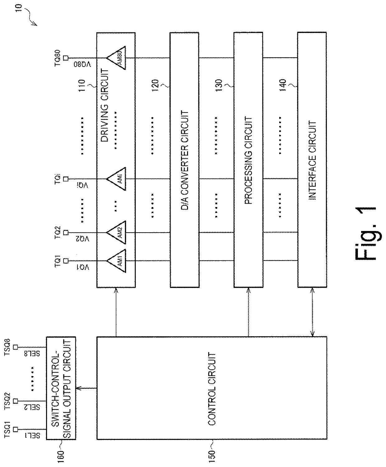
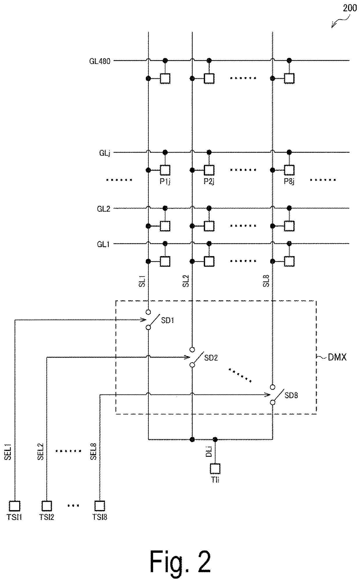
[0037]FIG. 1 illustrates an example configuration of a display driver 10. The display driver 10 includes a driving circuit 110 and a switch-control-signal output circuit 160. Furthermore, the display driver 10 may include a D / A converter circuit 120, a processing circuit 130, an interface circuit 140, a control circuit 150, image-signal output terminals TQ1 to TQ80, and switch-control-signal output terminals TSQ1 to TSQ8.

[0038]The interface circuit 140 establishes communication between an external processing device of the display driver 10 and the display driver 10. The proc...


PUM

PropertyMeasurementUnit
timeaaaaaaaaaa
timeaaaaaaaaaa
time constantaaaaaaaaaa

Abstract

A display driver includes an amplifier circuit configured to output time-sequentially arrayed first to n-th data voltages to an image-signal input terminal, and a switch-control-signal output circuit configured to output switch control signals that control the first to n-th switches disposed between the image-signal input terminal and respective first to n-th data lines. The switch-control-signal output circuit outputs the switch control signals that turn on two or more switches including a p-th switch (where p is an integer within the range of 2 to n, inclusive) among the first to n-th switches during a first driving period. The amplifier circuit outputs a p-th data voltage among the first to n-th data voltages during the first driving period.

Description

BACKGROUND1. Technical Field[0001]The present invention relates to a display driver, an electrooptic device, and an electronic apparatus.2. Related Art[0002]For an electrooptic apparatus, such as a liquid crystal display, there is known a pre-charge method of applying a predetermined pre-charge voltage to pixels before writing data voltage in the pixels. Pre-charge is carried out with the aim of, for example, writing assistance of a data voltage. In writing assistance of a data voltage, a pre-charge voltage similar to the data voltage scheduled to be written in a pixel is preliminarily applied to the pixel, to suppress insufficient writing of the data voltage (the difference between the actual voltage written in the pixel and the data voltage).[0003]As a known pre-charge technique, a technique is disclosed in, for example, JP-A-2012-37827. In JP-A-2012-37827, during a pre-charge period before writing a data voltage (image signal) in k pixels, an amplifier circuit applies a predeterm...

Claims


Application Information

Patent Timeline
Patent Type & Authority Patents(United States)
IPC IPC(8): G09G3/36G09G3/20G09G3/3258G02F1/133
CPCG09G3/3622G02F1/13306G09G3/2092G09G3/3258G09G2310/0251G09G2310/0291G09G2310/0297
Inventor BANSHO, RYOTA
Owner SEIKO EPSON CORP
Why Eureka
Try Eureka