

OLED display panel, manufacturing method of OLED display panel and display device
A display panel and one-sided technology, which is applied in semiconductor/solid-state device manufacturing, organic semiconductor devices, electrical components, etc., can solve the problem of large viewing angle deviation of OLED display panels, affect the display effect of OLED display panels, and product color mixing, etc., to achieve Alleviate the large-view role deviation, improve the display effect, and prevent the effect of product color mixing
- Summary
- Abstract
- Description
- Claims
- Application Information
AI Technical Summary
Problems solved by technology
Method used
Image

Examples
Embodiment 1
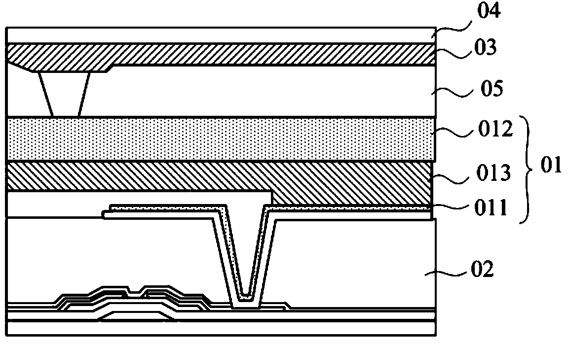
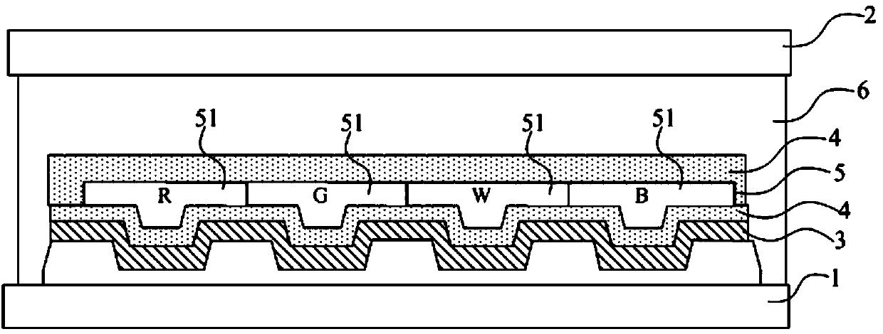
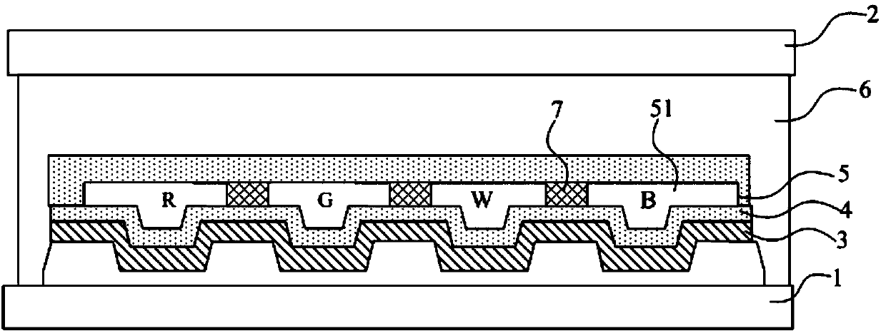
[0043] Please refer to figure 2 , is a structural schematic diagram of an OLED display panel provided in Embodiment 1 of the present invention, wherein the OLED display panel includes: an array substrate 1 and a packaging cover 2 arranged oppositely, and a side of the array substrate 1 facing the packaging cover 2 The OLED layer 3 also includes:
[0044] At least one thin film encapsulation layer 4, which covers the OLED layer 3 and is bonded to the array substrate 1;
[0045] The color filter layer 5 is located on the side of at least one thin-film encapsulation layer 4 facing the encapsulation cover plate 2;
[0046] The bonding adhesive material 6 is filled between the array substrate 1 and the packaging cover plate 2 to bond the array substrate and the packaging cover plate. The bonding adhesive material 6 covers the color filter layer 5 and the thin film packaging layer 4 .
[0047] In the OLED display panel provided in this embodiment, since at least one film encapsul...
Embodiment 2
[0068] Embodiment 2 provides a display device, which includes the OLED display panel provided in any one of the foregoing embodiments.
[0069] In the OLED display panel provided by the first embodiment above, the distance between the OLED layer 3 and the color filter layer 5 is relatively small, which can prevent the light emitted by the light-emitting area in the OLED layer 3 corresponding to a sub-pixel unit in the display panel. Irradiate on the color filter layer 5 of other sub-pixel units, so as to prevent the phenomenon of light mixing, and help to alleviate the problem of large viewing angle deviation in the OLED display panel; therefore, the display with the above-mentioned OLED display panel provided in this embodiment In the device, the problem of large viewing angle deviation in the OLED display panel can be effectively alleviated, thereby helping to increase the viewing angle of the display device provided in this embodiment and improving the display effect.
Embodiment 3
[0071] This embodiment provides a method for preparing the OLED display panel provided in the first embodiment above, such as Image 6 shown, including:
[0072] Step S601: forming an OLED layer including a plurality of organic light emitting diodes (OLEDs) on an array substrate;
[0073] Step S602: forming at least one thin film encapsulation layer on the OLED layer;
[0074] Step S603: forming a color filter layer on at least one thin film encapsulation layer;
[0075] Step S604: filling and laminating glue;
[0076] Step S605: Press-bonding the package cover to the bonding adhesive.
[0077] Based on the advantages of the above-mentioned OLED display panel, in the OLED display panel prepared by the preparation method provided by the present invention, the distance between the OLED layer and the color filter layer is relatively small, which can prevent the contact with a sub-color filter layer in the display panel. The light emitted by the light-emitting area of the OL...
PUM
 Abstract
Description
Claims
Application Information