

Display panel and manufacturing method thereof
A display panel and substrate technology, which is applied in semiconductor/solid-state device manufacturing, semiconductor devices, electrical components, etc., and can solve problems that affect viewing effects, image ghosting, discoloration, etc.
- Summary
- Abstract
- Description
- Claims
- Application Information
AI Technical Summary
Problems solved by technology
Method used
Image

Examples
Embodiment Construction
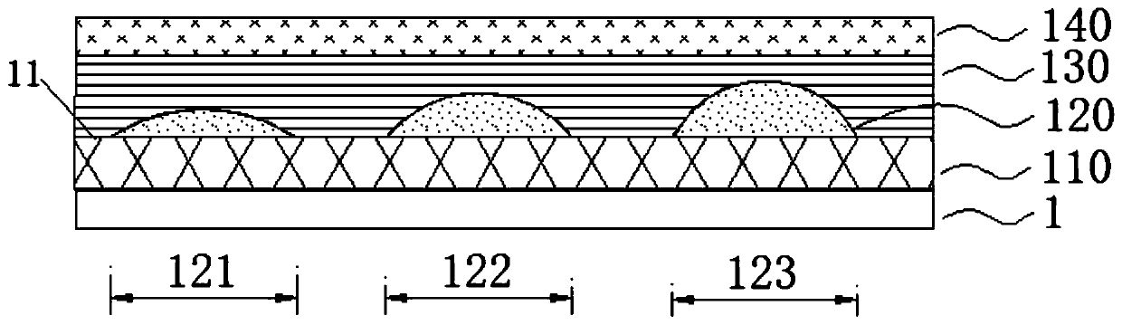
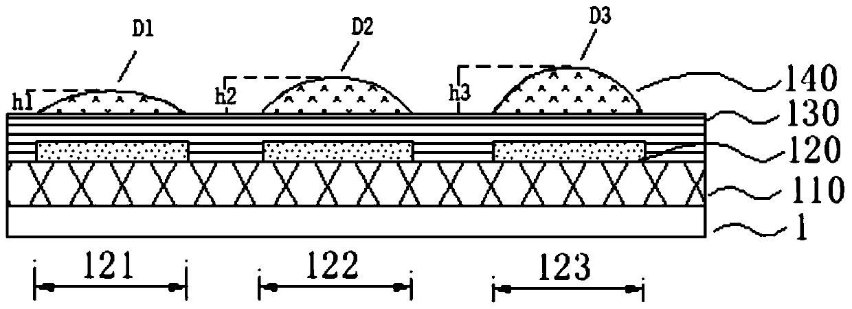
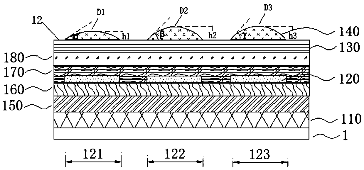
[0025] The present invention will be further described in detail below in conjunction with the accompanying drawings and embodiments. It should be understood that the specific embodiments described here are only used to explain the present invention, but not to limit the present invention. In addition, it should be noted that, for the convenience of description, only some structures related to the present invention are shown in the drawings but not all structures.
[0026] Due to the microcavity effect between the anode and cathode of the OLED device, there will be brightness attenuation and color shift under large viewing angles.
[0027] In order to solve the above problems, an embodiment of the present invention provides a display panel, by making the light-emitting film layer or the organic film layer located in the first pixel area, the second pixel area and the third pixel area have protrusions with different radians, so that The convex part can make the exit angle and ...
PUM
 Abstract
Description
Claims
Application Information