Light sensing chip, camera and electronic product
A technology of photosensitive chips and cameras, applied in TV, electrical components, color TV, etc., can solve the problems of smaller pixel area of photosensitive chips and higher and higher requirements for image quality, and achieve enhanced optical signal strength, reduced volume, and improved The effect of utilization
- Summary
- Abstract
- Description
- Claims
- Application Information
AI Technical Summary
Problems solved by technology
Method used
Image
Examples
Embodiment 1
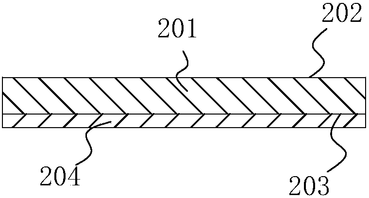
[0058] Such as figure 2 As shown, a photosensitive chip described in this embodiment includes a chip body 201. The chip body 201 has a light-receiving surface 202 for receiving light emitted from the lens direction to the chip body 201 and a backlight surface 203 opposite to the light-receiving surface 202. The surface 203 is coated with a reflective layer 204 capable of reflecting light emitted from the light-receiving surface through the chip body 201 back to the chip body 201 . The light-receiving surface 202 and the backlight surface 203 are arranged parallel to each other, so as to ensure that the trajectory of the light is the same when the light is emitted from the backlight surface 203, reflected by the reflective layer 204, and then injected into the backlight surface 203, so that the reflected light is on the chip body 201 The action point on the light receiving surface 202 is the same as that of the light incident on the light receiving surface 202 from the directi...
Embodiment 2
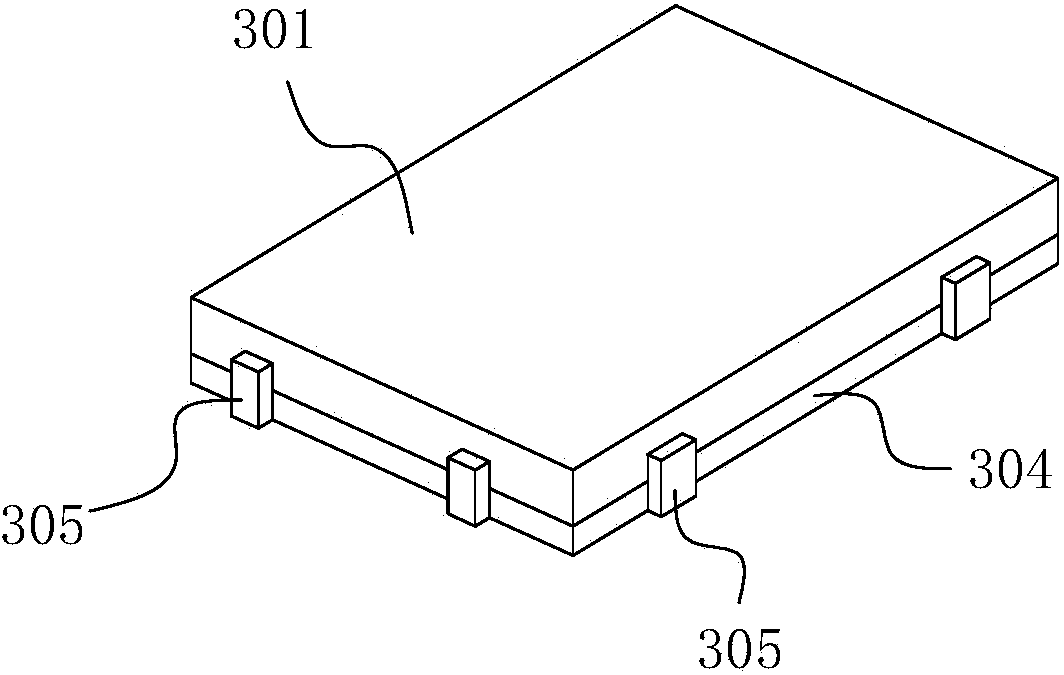
[0060] Such as image 3 , 4 As shown, a photosensitive chip described in this embodiment includes a chip body 301 having a light receiving surface 302 and a backlight surface 303 and a reflection device capable of reflecting light back to the chip body 301, wherein the reflection device is arranged on the backlight surface of the chip body 301 303 side. In this embodiment, the reflecting device is a layer of reflecting film 304. The chip body 301 and the reflecting film 304 have the same outline and corresponding dimensions. The connector 305 of the 304 film, the reflective film 304 is connected to the chip body 301 through the connector 305 and is tightly pasted on the backlight surface 303 of the chip body 301 .
Embodiment 3
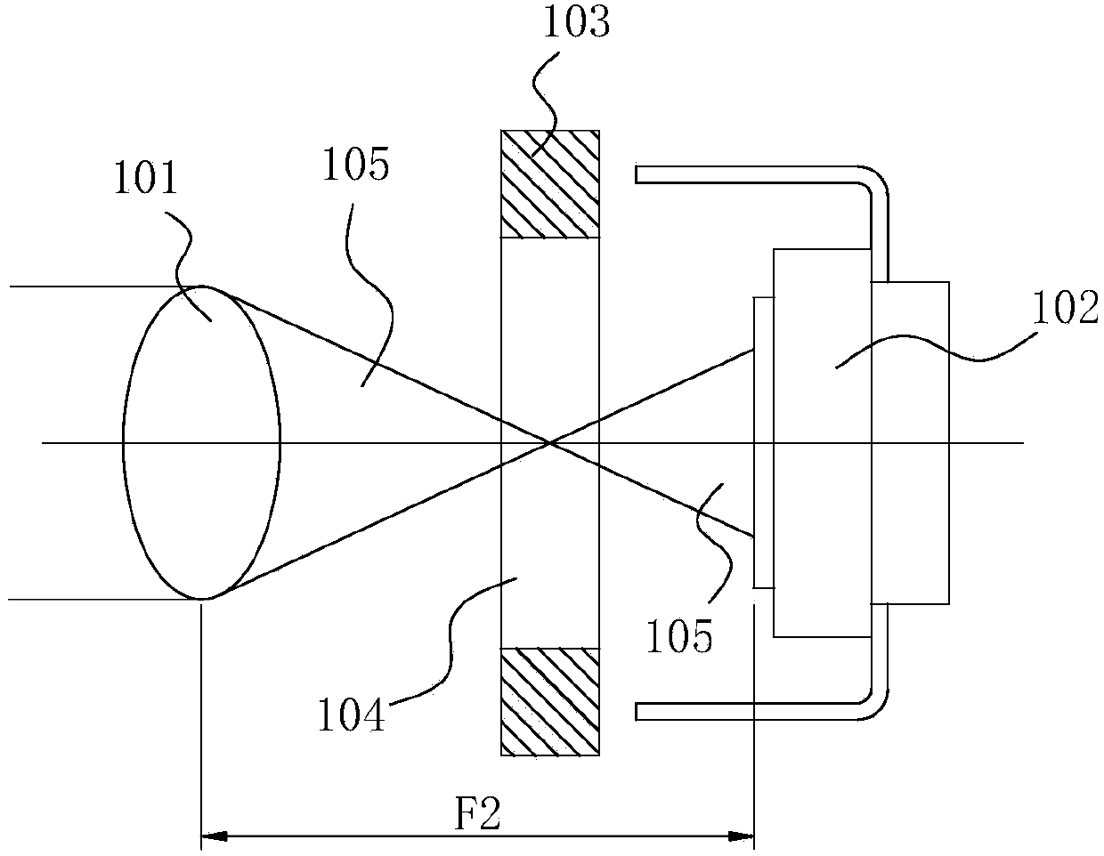
[0062] Such as Figure 5 , 6 , 7, a camera described in this embodiment includes a lens 401, a lens holder 402, and a circuit board 405 arranged sequentially from top to bottom (wherein up, down, and up and down in subsequent descriptions all refer to Direction), a light hole 403 is opened in the middle of the lens holder 402, a filter 404 is arranged above the light hole 403 and between the lens 401 and the lens holder 402, and the line corresponding to the position of the light hole 403 A photosensitive chip is arranged on the board 405, and the photosensitive chip includes a chip body 406. The upper surface of the chip body 406 is a light-receiving surface 407, and the lower surface is a backlight surface 408. The backlight surface 408 of the chip body 406 is coated with The light emitted by the body 406 from the light receiving surface 407 is reflected back to the reflective layer 409 of the chip body 406 .
PUM
 Abstract
Description
Claims
Application Information
 - R&D
- Intellectual Property
- Life Sciences
- Materials
- Tech Scout
- Unparalleled Data Quality
- Higher Quality Content
- 60% Fewer Hallucinations
Browse by: Latest US Patents, China's latest patents, Technical Efficacy Thesaurus, Application Domain, Technology Topic, Popular Technical Reports.
© 2025 PatSnap. All rights reserved.Legal|Privacy policy|Modern Slavery Act Transparency Statement|Sitemap|About US| Contact US: help@patsnap.com


