

Pixel test circuit for AMOLED
A technology for testing circuits and pixels, applied in static indicators, instruments, etc., can solve problems such as increasing the cost of supporting equipment, and achieve the effect of reducing the number of independent probes and reducing costs
- Summary
- Abstract
- Description
- Claims
- Application Information
AI Technical Summary
Problems solved by technology
Method used
Image

Examples
Embodiment Construction
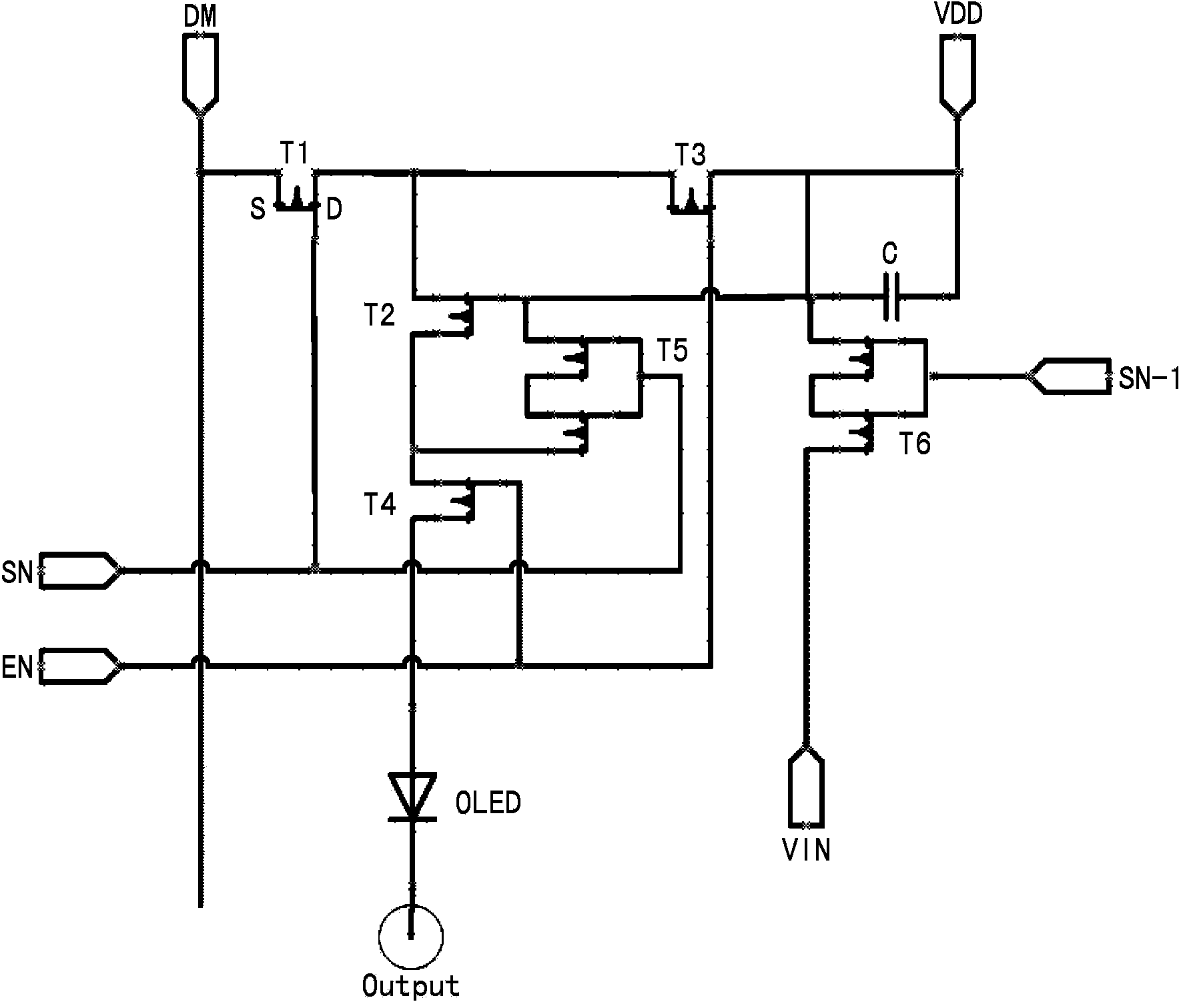
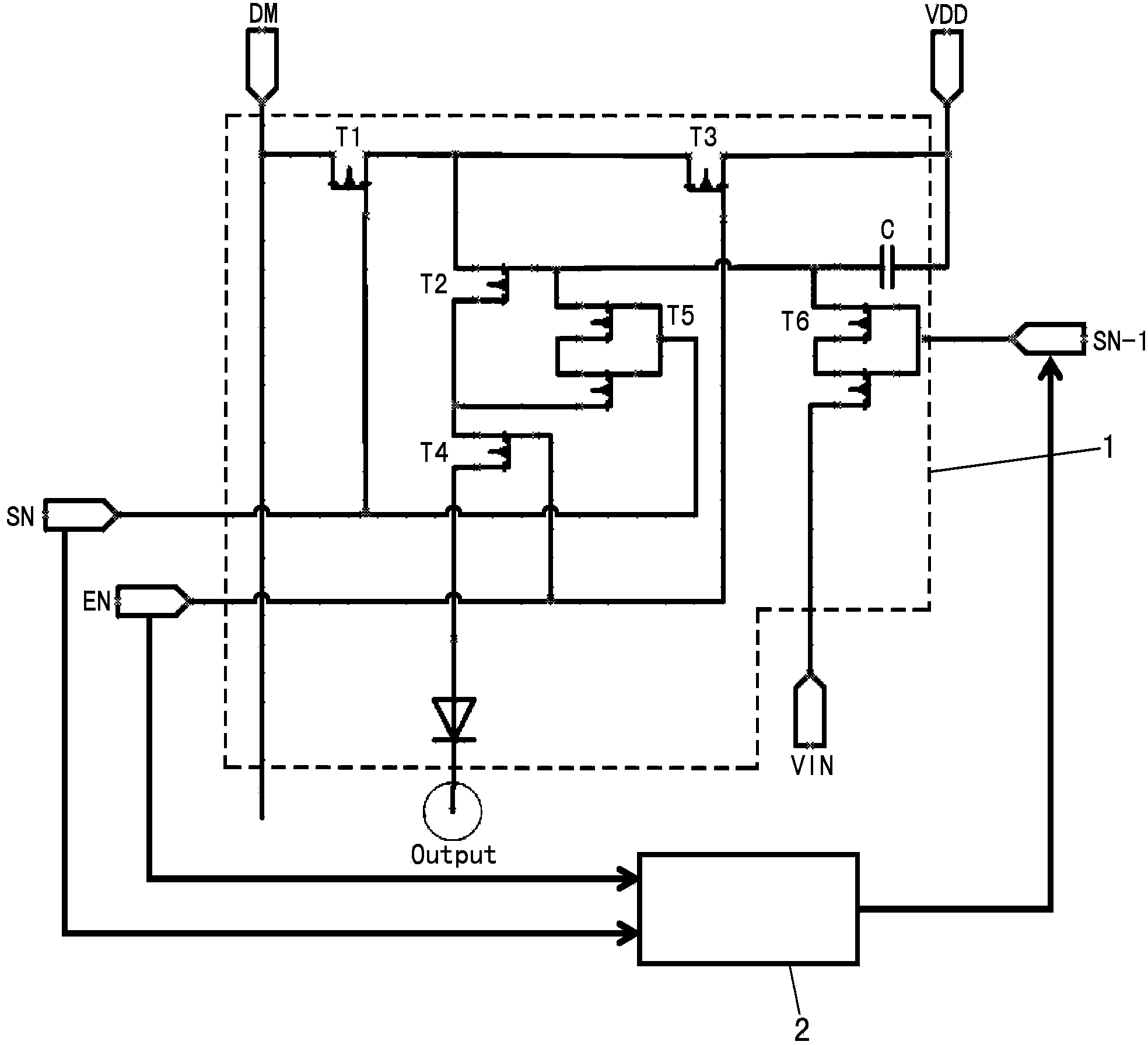
[0023] Hereinafter, embodiments of the present invention will be described in detail with reference to the drawings.
[0024] In the following drawings, the same reference numerals are attached to the same or corresponding parts, and repeated descriptions will be omitted.
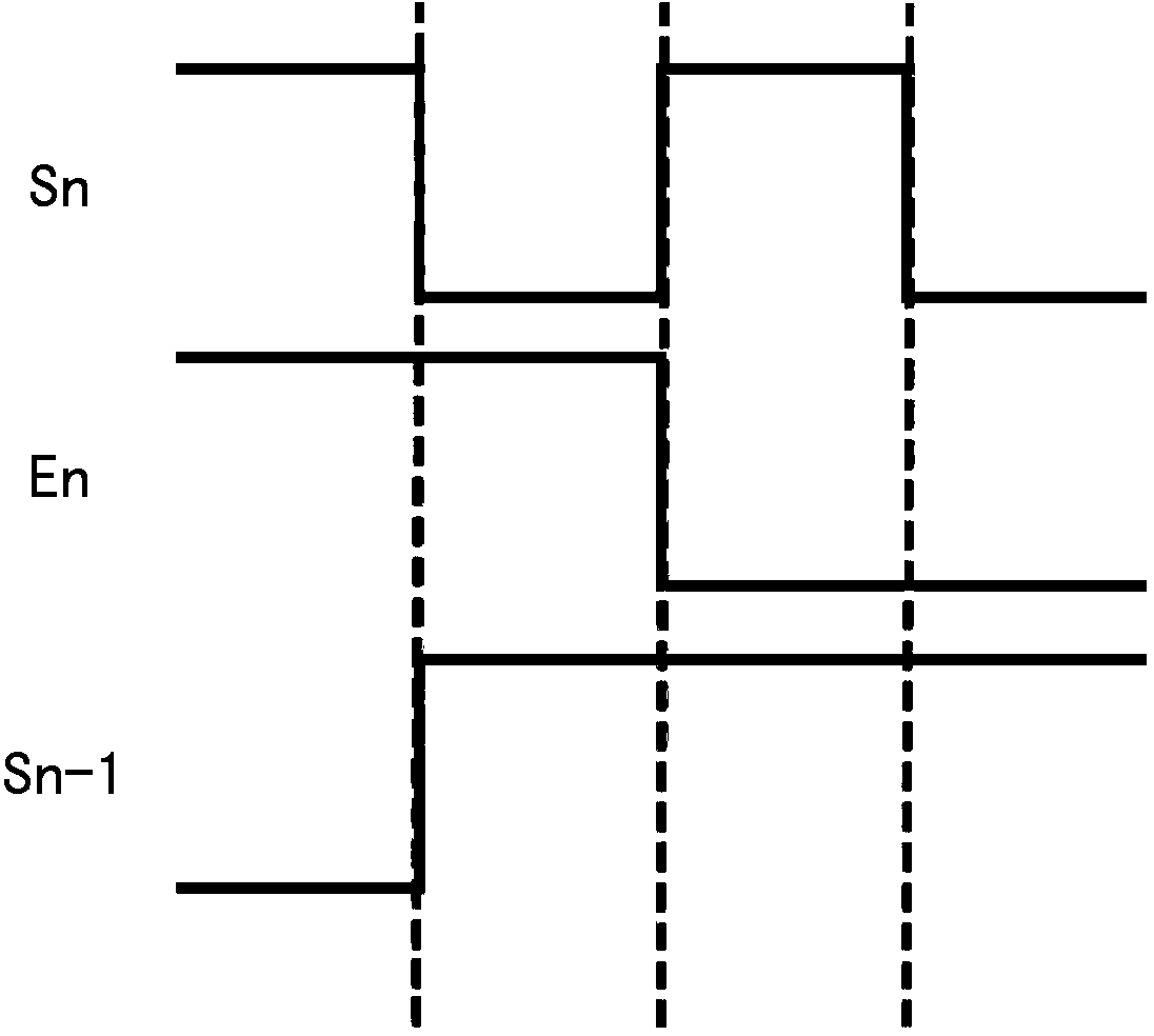
[0025] figure 2 yes means figure 1 The timing waveform diagram of the lighting control signal, the current scan signal and the front row scan signal of the pixel test circuit shown.
[0026] Such as figure 2 As shown, when the current scanning signal SN and the light-emitting control signal EN are both high level 1, the front row scanning signal SN-1 is low-level 0; when the current scanning signal SN is low-level 0, the light-emitting control signal EN is When the high level is 1, the front row scanning signal SN-1 is high level 1; when the current scanning signal SN is high level 1 and the light control signal EN is low level 0, the front row scanning signal SN-1 is high Level 1; when the current sc...
PUM
 Abstract
Description
Claims
Application Information