How to form a test line

A test line and test pattern technology, applied in the direction of electrical components, electric solid devices, circuits, etc., can solve the problems of small area, unable to make long test lines, etc., to achieve simple process, neat test pattern, easy to find. Effect

Active Publication Date: 2016-12-28
SEMICON MFG INT (SHANGHAI) CORP
View PDF4 Cites 0 Cited by
  • Summary
  • Abstract
  • Description
  • Claims
  • Application Information

AI Technical Summary

Problems solved by technology

However, with the improvement of the integration level of semiconductors, the utilization rate of semiconductor design on the wafer surface is getting higher and higher, resulting in smaller and smaller blank areas that can be used to make test lines.
The manufacturing method of the existing test line is usually realized by photolithography process. For example, the Chinese invention patent application with the publication number CN101894756A provides a "method for forming grooves, a method for forming metal wiring, photolithography method and equipment" , but limited by the resolution of the photolithography process, it is impossible to make a test line with a large length in a small area by using the photolithography process

Method used


Image

  • How to form a test line
  • How to form a test line
  • How to form a test line

Examples


Embodiment Construction

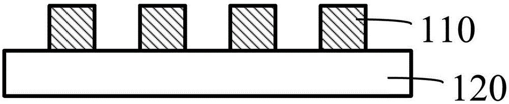
[0024] The manufacturing method of the existing test line is usually a photolithography process, and the corresponding test line is formed by steps such as exposure and development. Due to the influence of the resolution of the photolithography process, the line width of the test lines formed by the photolithography process is usually more than 400 angstroms, and the distance between two parallel test lines is more than 800 angstroms. Therefore, using the existing method to fabricate a test line has a low area utilization rate for the surface area of ​​the wafer, and it is impossible to fabricate a test line with a large length in an area with a small area.

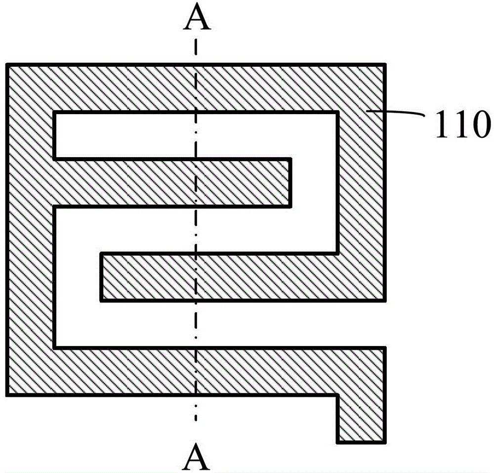
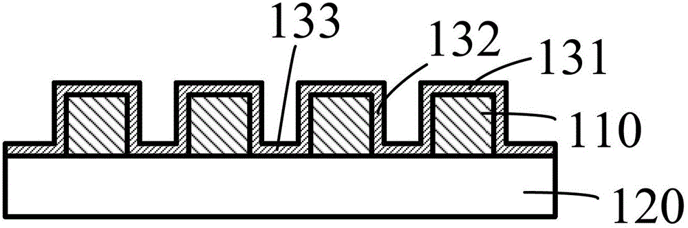
[0025] The present invention provides a method for manufacturing a test line, which comprises forming a first test pattern on a test material layer, then forming a first spacer on the sidewall of the test pattern, then removing the test pattern, and placing the first spacer on the sidewall of the test pattern. A notch is ...


PUM


Abstract

The present invention provides a method for forming a test line, comprising: providing a substrate with a test material layer; forming a first test pattern on the test material layer; forming a first side wall on the side wall of the first test pattern ; removing the first test pattern to form a first closed pattern; forming a first gap on the first closed pattern to form a second test pattern; forming a second side wall on the side wall of the second test pattern; removing the second test pattern to form a second closed pattern; forming a second gap on the second closed pattern to form a third test pattern; transferring the third test pattern to the test material layer to form a test pattern Wire. The method for forming the test line provided by the technical solution of the present invention can produce a test line with a relatively large length in an area with a small area, and the test line with a large length can be used to accurately test the resistivity of the material for making the test line. Therefore, it is beneficial to obtain accurate resistivity of the metal wire in the functional area.

Description

technical field [0001] The invention relates to the field of semiconductor technology, in particular to a method for forming a test line. Background technique [0002] In the semiconductor back-end process, test lines of a certain length are usually fabricated in a certain blank area of ​​the wafer surface. The test line is made of the same material as the metal lines (such as metal interconnect lines) in the functional area of ​​the semiconductor device. Its function is to replace the metal lines in the functional area to receive resistance value detection, and calculate the resistance value according to the detected resistance value. Test the resistivity of the wire to obtain the resistivity of the metal wire of the functional area. [0003] If the length of the test line is small, it is detected that the resistance value of the test line is unstable, and the accuracy of the resistivity obtained by the test line is low. For this reason, it is usually necessary to set the...

Claims


Application Information

Patent Timeline
Patent Type & Authority Patents(China)
IPC IPC(8): H01L23/544
Inventor 尚飞何其旸
Owner SEMICON MFG INT (SHANGHAI) CORP
Why Eureka
Try Eureka