Method, system and terminal equipment for testing epitaxial layer resistivity

A test method and epitaxial layer technology, which is applied in the direction of measuring resistance/reactance/impedance, measuring devices, measuring electrical variables, etc., can solve the problems of poor chip quality and inaccurate monitoring of epitaxial layer resistivity, etc., and achieve the effect of accurate measurement

Active Publication Date: 2021-04-27
HEBEI POSHING ELECTRONICS TECH
View PDF10 Cites 0 Cited by
  • Summary
  • Abstract
  • Description
  • Claims
  • Application Information

AI Technical Summary

Problems solved by technology

[0004] In view of this, the embodiment of the present invention provides a method, system and terminal equipment for testing the resistivity of the epitaxial layer to solve the current problem of poor chip quality due to inaccurate monitoring of the resistivity of the epitaxial layer

Method used


Image

  • Method, system and terminal equipment for testing epitaxial layer resistivity
  • Method, system and terminal equipment for testing epitaxial layer resistivity
  • Method, system and terminal equipment for testing epitaxial layer resistivity

Examples


Embodiment 1

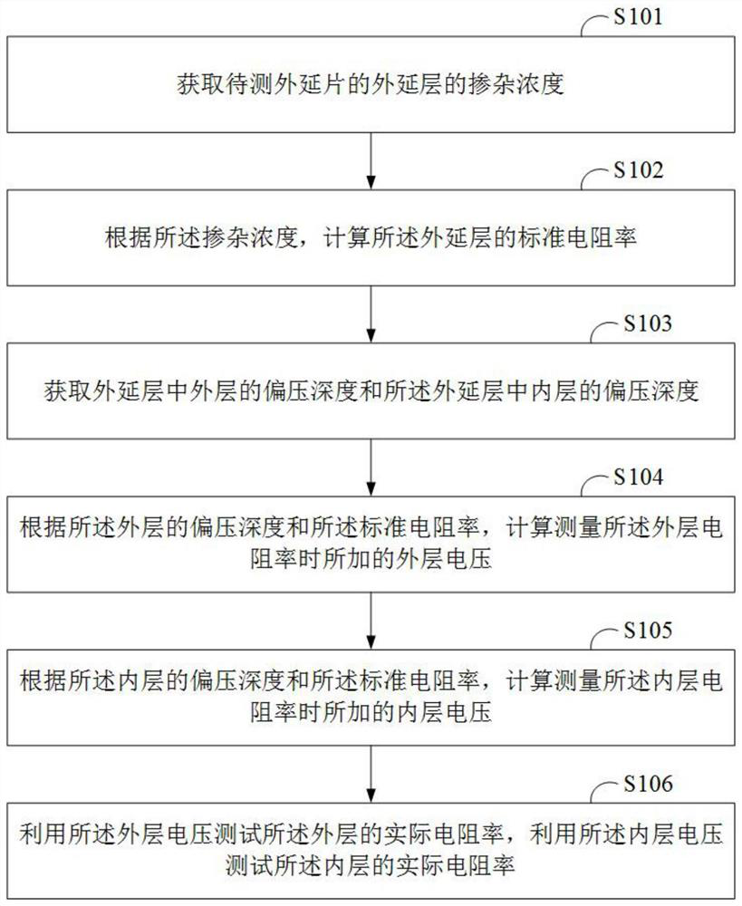
[0030] figure 1 It shows the implementation flowchart of the test method for the resistivity of the epitaxial layer provided by an embodiment of the present invention. For the convenience of explanation, only the parts related to the embodiment of the present invention are shown, and the details are as follows:

[0031] like figure 1 As shown, a method for testing the resistivity of an epitaxial layer provided by an embodiment of the present invention includes:

[0032] S101. Obtain the doping concentration of the epitaxial layer of the epitaxial wafer to be tested.

[0033] S102. Calculate a standard resistivity of the epitaxial layer according to the doping concentration.

[0034] S103. Obtain the bias depth of the outer layer in the epitaxial layer and the bias depth of the inner layer in the epitaxial layer, wherein the bias depth is a depth tested after voltage is applied to the epitaxial wafer.

[0035] S104. According to the bias depth of the outer layer and the stan...

Embodiment 2

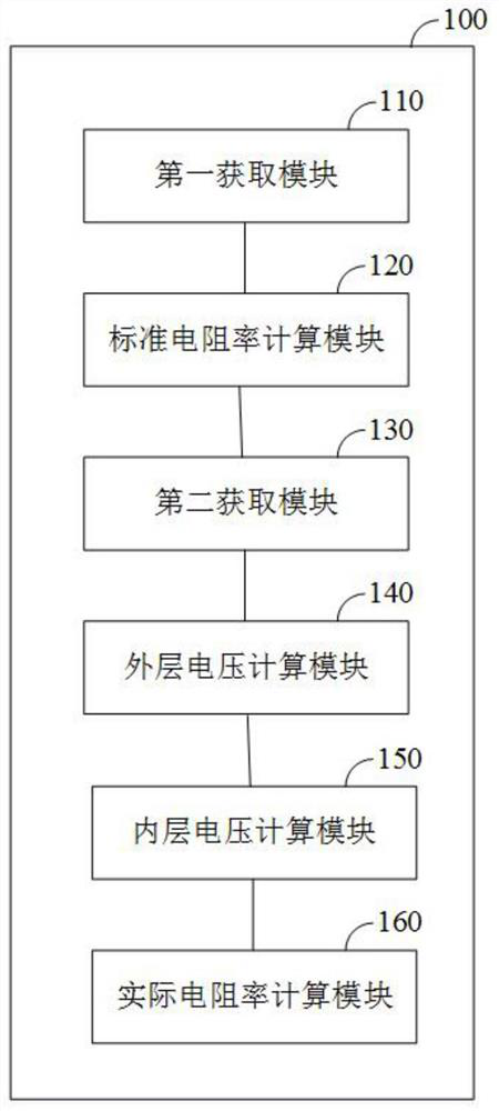
[0074] like figure 2 As shown, an embodiment of the present invention provides a system 100 for performing figure 1 The method step in the corresponding embodiment, it comprises:

[0075] The first obtaining module 110 is used to obtain the doping concentration of the epitaxial layer of the epitaxial wafer to be tested;

[0076] A standard resistivity calculation module 120, configured to calculate the standard resistivity of the epitaxial layer according to the doping concentration;

[0077] The second acquisition module 130 is configured to acquire the bias depth of the outer layer in the epitaxial layer and the bias depth of the inner layer in the epitaxial layer, wherein the bias depth is the depth tested after the voltage is applied to the epitaxial wafer;

[0078] The outer layer voltage calculation module 140 is used to calculate the outer layer voltage applied when measuring the outer layer resistivity according to the bias depth of the outer layer and the standard ...

Embodiment 3

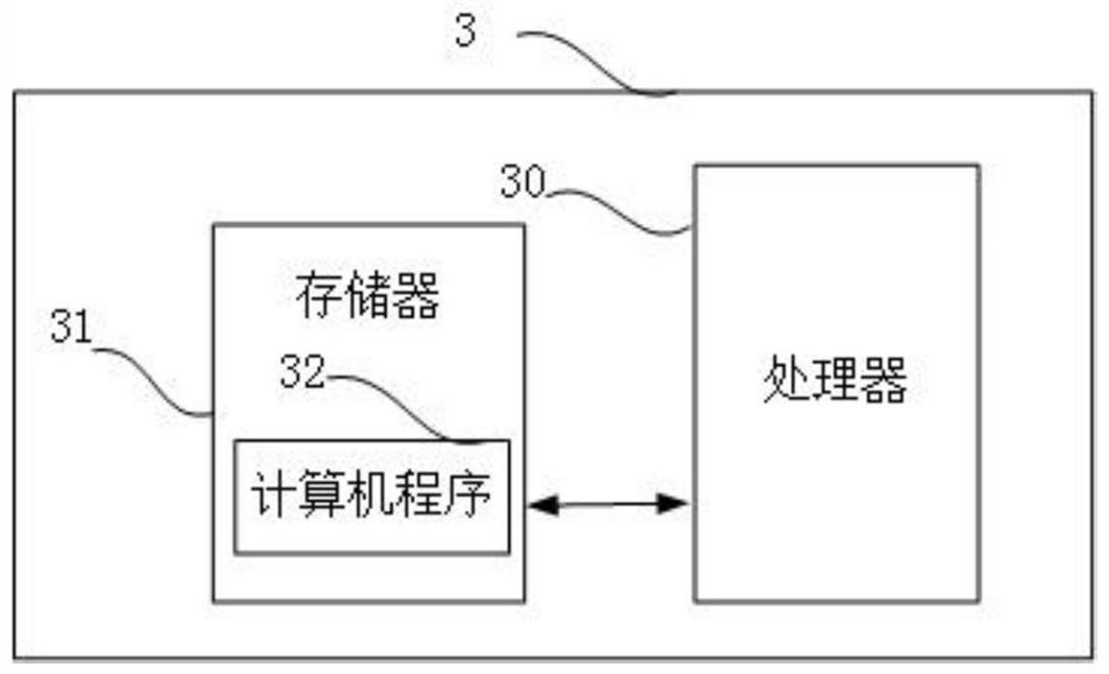
[0111] image 3 It is a schematic diagram of a terminal device provided by an embodiment of the present invention. like image 3 As shown, the terminal device 3 in this embodiment includes: a processor 30 , a memory 31 , and a computer program 32 stored in the memory 31 and operable on the processor 30 . When the processor 30 executes the computer program 32, it realizes the steps in each embodiment as described in Embodiment 1, for example figure 1 Steps S101 to S106 are shown. Alternatively, when the processor 30 executes the computer program 32, it realizes the functions of each module / unit in each system embodiment as described in Embodiment 2, for example figure 2 The functions of the modules 110 to 160 are shown.

[0112] The terminal device 3 refers to a terminal with data processing capabilities, including but not limited to computers, workstations, servers, and even smart phones with excellent performance, palmtop computers, tablet computers, personal digital assis...


PUM


Abstract

The invention provides a method, system and terminal equipment for testing the resistivity of an epitaxial layer. The method includes: obtaining the doping concentration of the epitaxial layer of the epitaxial wafer to be tested; and calculating the standard resistance of the epitaxial layer according to the doping concentration Obtain the bias depth of the outer layer in the epitaxial layer and the bias depth of the inner layer in the epitaxial layer; according to the bias depth and standard resistivity of the outer layer, calculate the outer layer voltage added when measuring the resistivity of the outer layer; According to the bias depth and standard resistivity of the inner layer, calculate the inner layer voltage applied when measuring the inner layer resistivity; use the outer layer voltage to test the actual resistivity of the outer layer, and use the inner layer voltage to test the actual resistivity of the inner layer. The invention can accurately measure the resistivity of the inner layer and the resistivity of the outer layer in the epitaxial layer respectively, thereby ensuring the quality of the chip.

Description

technical field [0001] The invention belongs to the technical field of epitaxial wafer detection, and in particular relates to a test method, system and terminal equipment for the resistivity of an epitaxial layer. Background technique [0002] The epitaxial process is widely used in bipolar integrated circuits, high voltage devices and CMOS integrated circuits. The core issue in mass production is the stability of product parameter control. In order to monitor the stability of parameters, it is necessary to regularly monitor the key parameter resistivity of the epitaxial layer. For the parameters of double-layer epitaxy, since the resistivity of the inner layer will also change due to the process fluctuation of the epitaxial furnace during the growth process, which will cause the deviation of the resistivity of the inner layer, it is necessary to monitor both the resistivity of the outer layer and the resistance of the inner layer. Rate. [0003] The conventional testing ...

Claims


Application Information

Patent Timeline
Patent Type & Authority Patents(China)
IPC IPC(8): G01R27/02
CPCG01R27/02
Inventor 张佳磊薛宏伟任丽翠
Owner HEBEI POSHING ELECTRONICS TECH
Why Eureka
Try Eureka