CMOS image sensor and line noise correction method thereof

An image sensor and correction method technology, applied in the field of image sensors, can solve problems such as line noise, and achieve the effects of line noise reduction and image quality improvement

Active Publication Date: 2014-10-29
思特威(上海)电子科技股份有限公司
View PDF9 Cites 17 Cited by
  • Summary
  • Abstract
  • Description
  • Claims
  • Application Information

AI Technical Summary

Problems solved by technology

[0007] The purpose of the present invention is to provide a CMOS image sensor and its line noise correction method, to solve the problem of line noise in the CMOS image sensor in the prior art

Method used


Image

  • CMOS image sensor and line noise correction method thereof
  • CMOS image sensor and line noise correction method thereof
  • CMOS image sensor and line noise correction method thereof

Examples


Embodiment Construction

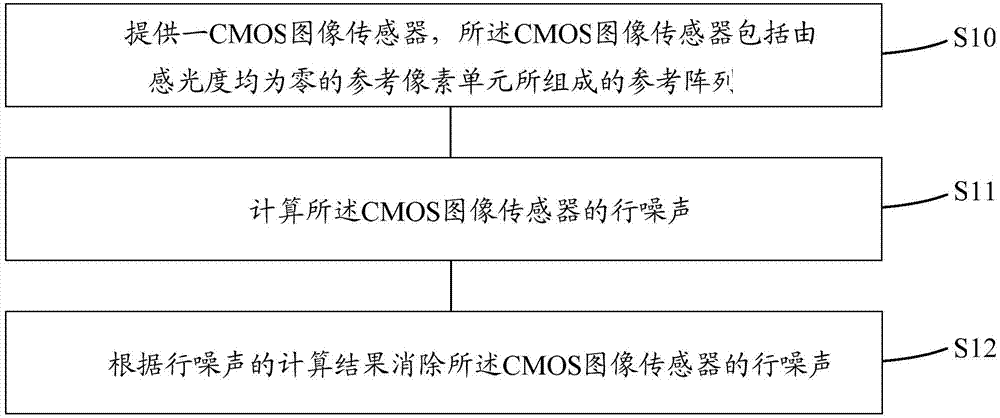
[0029] The CMOS image sensor and its line noise correction method proposed by the present invention will be further described in detail below with reference to the accompanying drawings and specific embodiments. Advantages and features of the present invention will be apparent from the following description and claims. It should be noted that all the drawings are in a very simplified form and use imprecise scales, and are only used to facilitate and clearly assist the purpose of illustrating the embodiments of the present invention.

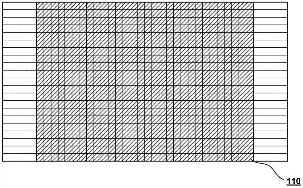
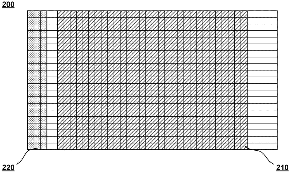
[0030] Please refer to figure 2 , which is a schematic structural diagram of a CMOS image sensor according to an embodiment of the present invention. Such as figure 2 As shown, the CMOS image sensor 200 includes a readout circuit (not shown), a pixel array 210 and a reference array 220; the pixel array 210 and the reference array 220 are respectively composed of a plurality of effective pixel units and a plurality of reference pixels The plu...


PUM


Abstract

The invention provides a CMOS image sensor and a line noise correction method thereof. The CMOS image sensor comprises a reading circuit, a pixel array and a reference array. The pixel array and the reference array are respectively composed of a plurality of effective pixel units and a plurality of reference pixel units, and the effective pixel units and the reference pixel units are electrically connected with a power supply and the reading circuit, wherein the light sensitivity of the reference pixel units is zero. The CMOS image sensor is provided with the reference array on the basis of the pixel array, each pixel unit of the reference array serves as the reference pixel unit, line noise can be calculated by reading output values of the reference pixel units, so that reduction of the line noise is achieved, and image quality of the CMOS image sensor is improved.

Description

technical field [0001] The invention relates to the technical field of image sensors, in particular to a CMOS image sensor and a line noise correction method thereof. Background technique [0002] A CMOS image sensor is a semiconductor device that converts an optical image into an electrical signal by using a photoelectric effect. The CMOS image sensor has a simple structure and high reliability, and thus has been widely used in many fields. [0003] Please refer to figure 1 , which is a schematic structural diagram of a CMOS image sensor in the prior art. Such as figure 1 As shown, the existing CMOS image sensor 100 includes a pixel array 110 and a readout circuit (not shown in the figure), and each pixel unit of the pixel array 110 is electrically connected to the power supply and the readout circuit respectively. [0004] When external light is irradiated on the pixel array 110 of the CMOS image sensor 100 , the photoelectric effect occurs in the pixel units of the pix...

Claims


Application Information

Patent Timeline
Patent Type & Authority Applications(China)
IPC IPC(8): H04N5/374H04N5/357
Inventor 王毫杰徐辰
Owner 思特威(上海)电子科技股份有限公司
Why Eureka
Try Eureka