Large current printed circuit board and machining method thereof

A printed circuit board and processing method technology, which is applied in the direction of assembling printed circuits with electrical components, printed circuits connected with non-printed electrical components, printed circuit components, etc., can solve signal line interference, increase wiring complexity, and improve reliability. Sexual hazards, etc.

Inactive Publication Date: 2014-10-29
SHENNAN CIRCUITS
View PDF6 Cites 1 Cited by
  • Summary
  • Abstract
  • Description
  • Claims
  • Application Information

AI Technical Summary

Problems solved by technology

[0003] At present, such PCBs carrying large currents usually use conductor blocks carrying high currents to be directly embedded in the circuit layer (wherein, the conductor blocks carrying high currents can be referred to as high-current conductor blocks, and the large-current conductor blocks are, for example, copper block) way to carry a large current, the inner layer circuit is connected to the large current conductor block through the outer layer circuit, so the complexity of the wiring is increased, and a large current needs to be carried between the circuit layers, which not only takes up more space on the outer layer for wiring , and there are certain hidden dangers in terms of reliability; the outer line needs to carry a large current, and the current conduction has certain interference and influence on other signal lines

Method used


Image

  • Large current printed circuit board and machining method thereof
  • Large current printed circuit board and machining method thereof
  • Large current printed circuit board and machining method thereof

Examples


Embodiment Construction

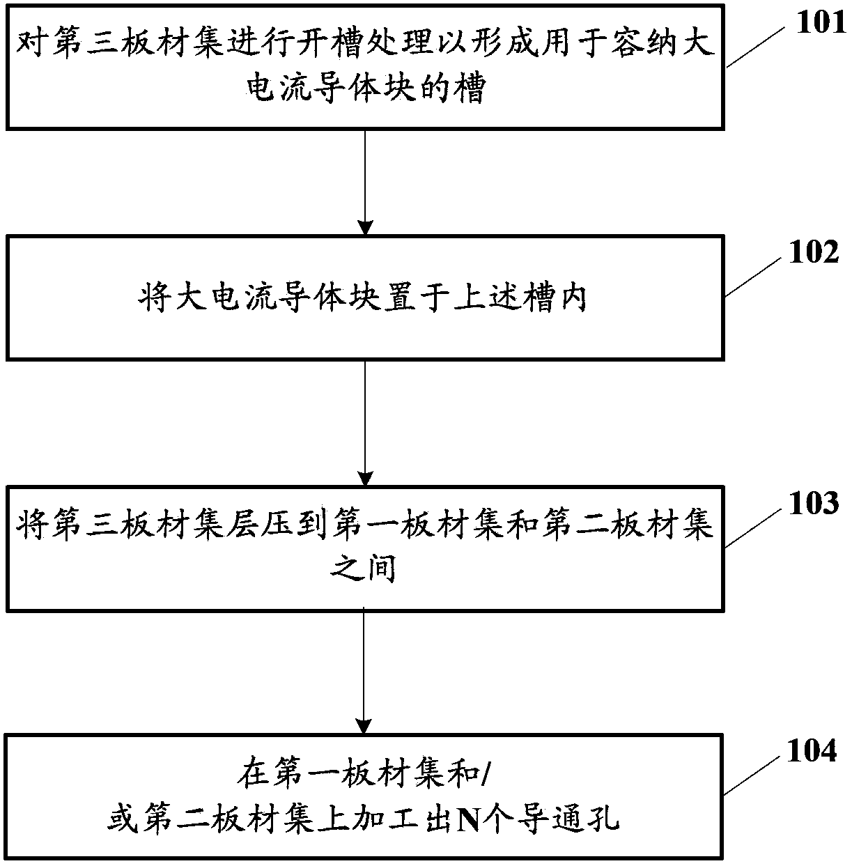
[0030] The embodiments of the present invention provide a high-current printed circuit board and a processing method thereof, in order to improve the reliability of the PCB and reduce wiring complexity and interference.

[0031] In order to enable those skilled in the art to better understand the solutions of the present invention, the following will clearly and completely describe the technical solutions in the embodiments of the present invention in conjunction with the drawings in the embodiments of the present invention. Obviously, the described embodiments are only It is an embodiment of a part of the present invention, but not all embodiments. Based on the embodiments of the present invention, all other embodiments obtained by persons of ordinary skill in the art without making creative efforts shall fall within the protection scope of the present invention.

[0032] Each will be described in detail below.

[0033] The terms "first", "second", "third", "fourth", etc. (i...


PUM


Abstract

An embodiment of the invention discloses a large current printed circuit board and a machining method thereof. The machining method of the large current printed circuit board comprises slotting a third panel set to form into a groove which is used for accommodating a large current conductor block; arranging the large current conductor block into the groove; arranging the third panel set between a first panel set and a second panel set; machining N conducting holes in the first panel set and or the second panel set, wherein the third panel set comprises at least one layer of circuit graphic layer, every conducting hole of the N conducting holes is respectively in contact with the large current conductor block and the at least one layer circuit graphic layer in the third panel set to enable the large current conductor block and the at least one layer circuit graphic layer in the third panel to be connected and conducted. According to the technical scheme, the machining method of the large current printed circuit board enables improvement of the reliability of the PCB (Printed Circuit Board) to be facilitated and reduces wiring complexity and signal interference.

Description

technical field [0001] The invention relates to the field of circuit board production, in particular to a processing method of a high-current printed circuit board and a high-current printed circuit board. Background technique [0002] In many scenarios, high-power printed circuit boards (PCB, Printed Circuit Board) are required, such as high-power power amplifier PCBs, automotive electronics PCBs, and other electronic products that require high current (such as current > 5A or 30A) and signals. [0003] At present, such PCBs carrying large currents usually use conductor blocks carrying high currents to be directly embedded in the circuit layer (wherein, the conductor blocks carrying high currents can be referred to as high-current conductor blocks, and the large-current conductor blocks are, for example, copper block) way to carry a large current, the inner layer circuit is connected to the large current conductor block through the outer layer circuit, so the complexity ...

Claims


Application Information

Patent Timeline
Patent Type & Authority Applications(China)
IPC IPC(8): H05K3/32H05K3/40H05K3/46H05K1/02H05K1/11H05K1/18
Inventor 刘宝林郭长峰罗斌
Owner SHENNAN CIRCUITS
Why Eureka
Try Eureka