Display baseplate as well as manufacture method thereof and display device

A technology for display substrates and manufacturing methods, which is applied in the fields of instruments, nonlinear optics, optics, etc., and can solve problems such as inconsistent orientation of alignment layers, light leakage in dark states, and affecting device display quality

Active Publication Date: 2014-12-03
BOE TECH GRP CO LTD
View PDF8 Cites 10 Cited by
  • Summary
  • Abstract
  • Description
  • Claims
  • Application Information

AI Technical Summary

Problems solved by technology

In actual manufacturing, the inventors found that, limited by the technical level, there will inevitably be defects such as local orientation inco...

Method used


Image

  • Display baseplate as well as manufacture method thereof and display device
  • Display baseplate as well as manufacture method thereof and display device
  • Display baseplate as well as manufacture method thereof and display device

Examples


Embodiment 1

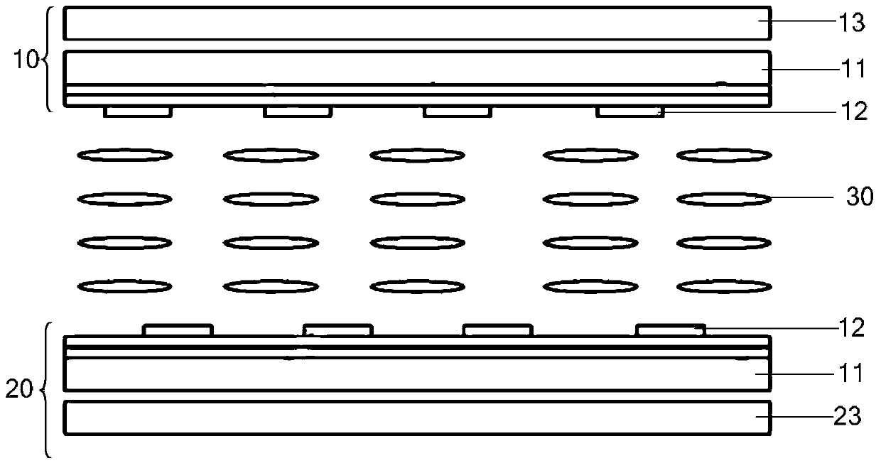
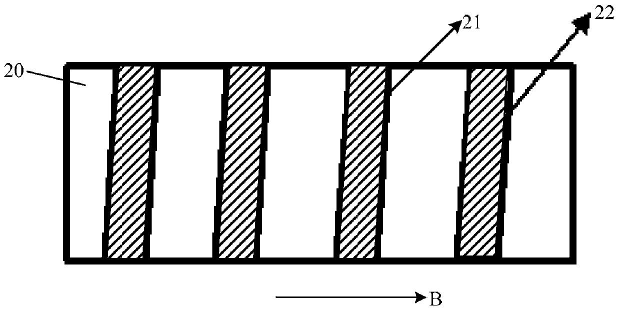
[0033] An embodiment of the present invention provides a display substrate. The display substrate is provided with: a blue-phase liquid crystal layer; and driving electrodes for driving the blue-phase liquid crystal layer in a dark state. Each group of driving electrodes includes two There are two opposite electrodes, and the components of the electric field generated by the two opposite electrodes in the blue phase liquid crystal layer in the first direction are not zero, and the first direction is perpendicular to the polarization direction of the incident light.

[0034] An embodiment of the present invention provides a display substrate, which is suitable for a flat field display device. The flat field display device mentioned here means that the electric field used to drive liquid crystal deflection for display is a parallel electric field parallel to the substrate. At present, there are mainly: plane switching technology (In-Plane Switching, referred to as IPS), Advanced ...

Embodiment 2

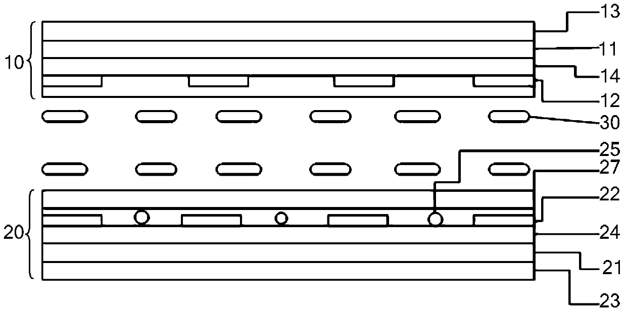
[0052] Embodiments of the present invention also provide a method for manufacturing a display substrate, such as Figure 5 As shown, the substrate manufacturing method also includes:

[0053] 101. The process of forming a blue phase liquid crystal layer;

[0054] 102. A process of forming driving electrodes, the driving electrodes are used to drive the blue-phase liquid crystal layer in a dark state, each group of driving electrodes includes two electrodes of the opposite sex, and the two electrodes of the opposite sex are in the blue phase The component of the electric field generated by the phase liquid crystal layer in the first direction is not zero, and the first direction is perpendicular to the polarization direction of the incident light.

[0055] The embodiment of the present invention also provides a method for manufacturing a display substrate. On the basis of the original process, the additional steps 101 and 102 of forming the blue phase liquid crystal layer and ...


PUM


Abstract

The embodiment of the invention discloses a display baseplate as well as a manufacture method thereof and a display device, and relates to the field of display. Dark state light leak can be reduced; the display quality of the device can be improved. The display baseplate is provided with a blue phase liquid crystal layer and driving electrodes used for driving the blue phase liquid crystal layer in the dark state; each group of driving electrodes comprises two out-of-phase electrodes; the component in a first direction of electric field generated by the two out-of-phase electrodes on the blue phase liquid crystal layer is not zero; the first direction is perpendicular to the polarization direction of incident light.

Description

technical field [0001] The invention relates to the display field, in particular to a display substrate, a manufacturing method thereof, and a display device. Background technique [0002] Advanced-Super Dimensional Switching (abbreviation: ADS) forms a multi-dimensional electric field through the parallel electric field generated by the edge of the pixel electrode or the common electrode in the same plane and the vertical electric field generated between the pixel electrode and the common electrode, so that the liquid crystal cell All alignment liquid crystal molecules between the inner pixel electrodes or the common electrodes, and directly above the pixel electrodes or the common electrodes can produce rotation conversion, thereby improving the working efficiency of the plane alignment liquid crystal and increasing the light transmission efficiency. Advanced ultra-dimensional field switching technology can improve the picture quality of TFT-LCD, and has the advantages of ...

Claims


Application Information

Patent Timeline
IPC IPC(8): G02F1/1343G02F1/1333
CPCG02F1/13471G02F1/13793G02F1/134309G02F1/137G02F1/1337G02F1/13439G02F1/1341G02F1/134363
Inventor 李明超
Owner BOE TECH GRP CO LTD
Why Eureka
Try Eureka