VA liquid crystal display screen and manufacturing method thereof

A technology for a liquid crystal display screen and a manufacturing method, which is applied in nonlinear optics, instruments, optics, etc., can solve problems such as blind areas of reverse viewing angle display, and achieve the effects of fast response speed, wide operating temperature range and high production efficiency

Active Publication Date: 2014-12-10
CONHUI HUIZHOU SEMICON
View PDF6 Cites 4 Cited by
  • Summary
  • Abstract
  • Description
  • Claims
  • Application Information

AI Technical Summary

Problems solved by technology

[0003] In the prior art, the COM electrode (common electrode) and SEG electrode (scanning electrode) in the VA liquid crystal display are designed using solid ITO, and these two electrodes achieve the design display viewing angle by specifying the friction viewing angle and the overlapping of electrodes range, but the disadvantage of this design is: there is a blind area of ​​the display in the area of ​​around 20° inverse viewing angle
Due to the above-mentioned limitations in the range of viewing angles of traditional VA products, how to eliminate the blind area of ​​anti-viewing angles and realize full viewing angles has become a new research topic for VA product designers and developers.

Method used


Image

  • VA liquid crystal display screen and manufacturing method thereof
  • VA liquid crystal display screen and manufacturing method thereof
  • VA liquid crystal display screen and manufacturing method thereof

Examples


Embodiment 1

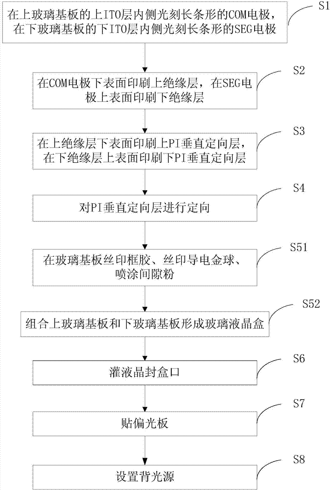
[0049] Such as figure 1 Shown, a kind of manufacture method of VA LCD comprises the following steps:

[0050]S1 photolithographic electrodes on the glass substrate. Specifically, a strip-shaped COM electrode is photoetched inside the upper ITO layer of the upper glass substrate, and a strip-shaped SEG electrode is photo-etched inside the lower ITO layer of the lower glass substrate, and several first electrodes are arranged in the COM electrode. Hollow structure, several second hollow structures are arranged in the SEG electrode. Both the first hollow structure and the second hollow structure are regular-shaped structures. For example, the plurality of first hollow structures in the COM electrode and the plurality of second hollow structures in the SEG electrode are any one of straight line shape, right angle shape, rhombus shape, rectangle shape, and triangle shape.

[0051] S2 printing an insulating layer on the electrode surface. Specifically, an upper insulating layer ...

Embodiment 2

[0066] Present embodiment except following feature other structures are with embodiment 1:

[0067] The step S4 specifically adopts rubbing orientation, using cotton cloth or nylon cloth as the rubbing cloth, wherein the density of the rubbing cloth is 24000 pieces / cm 2 ~6000pcs / cm 2 , the friction angle formed by the upper glass substrate and the lower glass substrate with the friction wheel is 0°~45°, the friction pressure is 0.1mm~0.6mm, the friction wheel speed is 500rpm~1200rpm, and the platform speed is 20mm / sec~60mm / sec.

Embodiment 3

[0069] Such as Figure 5 As shown, a VA liquid crystal display includes an upper glass substrate 1, frame glue 2, lower glass substrate 3, and gap powder 4, wherein the upper glass substrate and the lower glass substrate are fixed by frame glue and gap powder to form a glass liquid crystal cell. An upper ITO layer 5 is arranged below the upper glass substrate, an ITO layer 6 is arranged above the lower glass substrate, and a VA negative liquid crystal layer 7 is arranged between the upper ITO layer and the lower ITO layer. The gap powder is sprayed in the VA negative liquid crystal layer. An upper polarizer 14 and a lower polarizer 15 are provided on the outer sides of the upper glass substrate and the lower glass substrate, respectively. The inner side of the upper ITO layer is photolithographically strip-shaped COM electrode 8, the inner side of the lower ITO layer is photolithographically strip-shaped SEG electrode 9, and the COM electrode and the SEG electrode are orthogo...


PUM

PropertyMeasurementUnit
wavelengthaaaaaaaaaa
surface tensionaaaaaaaaaa
thicknessaaaaaaaaaa

Abstract

The invention relates to a VA liquid crystal display screen and a manufacturing method thereof. The method comprises the steps that a long-strip-shaped COM electrode is subjected to photoetching on the inner side of an upper ITO layer of an upper glass substrate, a long-strip-shaped SEG electrode is subjected to photoetching on the inner side of a lower ITO layer of a lower glass substrate, a plurality of first hollow-out structures are arranged in the COM electrode, a plurality of second hollow-out structures are arranged in the SEG electrode; an upper insulation layer is printed on the lower surface of the COM electrode, and a lower insulation layer is printed on the upper surface of the SEG electrode; and the upper glass substrate and the lower glass substrate are fixed to form a glass liquid crystal cell through frame glue and gap powder, the COM electrode and the SEG electrode are arranged in an orthogonality-overlapping mode, and the first hollow-out structures in the COM electrode and the second hollow-out structures in the SEG electrode are arrayed in parallel at intervals at equal distance. An anti-view-angle blind zone is removed, and a full-view-angle displaying effect is achieved.

Description

technical field [0001] The invention relates to the technical field of liquid crystal display screens, in particular to a VA liquid crystal display screen and a manufacturing method thereof. Background technique [0002] Traditional negative display LCDs use twisted nematic display technology. Existing negative LCD screens include TN / ETN / HTN / STN / FSTN / ESTN and other products. With the improvement of living standards and the development of science and technology, consumers have higher and higher requirements for liquid crystal display screens of products such as electronic products or home appliances. For example, the requirements for the range of display viewing angles of liquid crystal display screens are getting wider and wider. Therefore, VA liquid crystal display screens are favored by consumers because of their large viewing angles. [0003] In the prior art, the COM electrode (common electrode) and SEG electrode (scanning electrode) in the VA liquid crystal display ar...

Claims


Application Information

Patent Timeline
Patent Type & Authority Applications(China)
IPC IPC(8): G02F1/1343G02F1/1333G02F1/139
Inventor 王海曾新勇
Owner CONHUI HUIZHOU SEMICON
Why Eureka
Try Eureka