Scanning signal producing circuit

A technology for scanning signals and generating circuits, which can be applied to instruments, static indicators, etc., and can solve problems such as unsatisfactory narrow frame design of the display, abnormal circuits, abnormal display of the display, etc.

Active Publication Date: 2014-12-10
EVERDISPLAY OPTRONICS (SHANGHAI) CO LTD
View PDF7 Cites 9 Cited by
  • Summary
  • Abstract
  • Description
  • Claims
  • Application Information

AI Technical Summary

Problems solved by technology

[0005] First, whether the scanning signal output generated by the scanning signal generating circuit is mainly controlled by the transistor M1, since there is only one transistor M1 as the output of the scanning signal, and it is always in the conduction state, so the transistor M1 The function will decline, and when the transistor M1 is abnormal, it will cause the entire circuit to be abnormal, and then the display will be abnormal
[0006] Second, the pre-scanning signal generating circuit must be composed of eight transistors and two capacitors C1 and C2, so too many transistors will cause the space required for the scanning signal generating circuit to become larger, which cannot meet the narrow frame design of the display In addition, the excessive number of transistors also reduces the production yield

Method used


Image

  • Scanning signal producing circuit
  • Scanning signal producing circuit
  • Scanning signal producing circuit

Examples


Embodiment Construction

[0024] The present invention will be further described in detail below in conjunction with the accompanying drawings and specific embodiments.

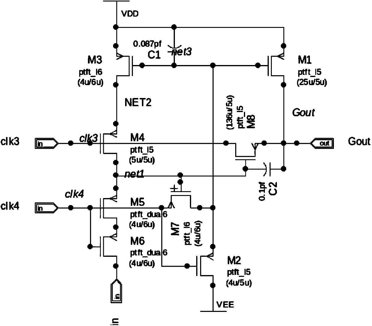
[0025] refer to figure 2 As shown, it is a scanning signal generation circuit provided by the embodiment of the present invention, which mainly consists of a first transistor M1, a second transistor M2, a first capacitor C1, a third transistor M3, and a fourth transistor M4 , a fifth transistor M5, and a second capacitor C2, and the first transistor M1 to the fifth transistor M5 are all P-type thin film transistors (Thin-Film Transistor, referred to as TFT), wherein:

[0026] The first transistor M1 has a first end 11 for receiving a data signal STV, a first control end 12 for receiving a second frequency signal CK2, and a first end 12 electrically connected to a first node NET1. The second terminal 13; in this embodiment, the first control terminal 12 of the first transistor M1 is a gate terminal and is used to control the conducti...


PUM


Abstract

The invention discloses a scanning signal producing circuit. The scanning signal producing circuit is mainly formed by five transistors which are matched with two capacitors, a scanning signal can be produced by means of few transistors, the setting space of the scanning signal producing circuit can be reduced so that the requirement of a narrow bezel design of a displayer can be met, meanwhile, two transistors of the scanning signal producing circuit perform outputting of the scanning signal by turns, and therefore, the stability of the scanning signal producing circuit can be improved.

Description

technical field [0001] The invention relates to a scanning signal generating circuit, in particular to a scanning signal generating circuit with two transistors outputting scanning signals in turn. Background technique [0002] With the development of display technology, the current display design trend is towards larger size, higher resolution, narrower frame and 3D display. [0003] In terms of the narrow bezel design direction, the original bezel of the display is mainly used as a storage area for chips and circuits. Therefore, simplifying the design of the scanning signal generation circuit in the bezel can greatly reduce the bezel width. However, how to On the basis of simplifying the scanning signal generating circuit, it is the most important development engine of the present invention to maintain a stable output scanning signal function. [0004] refer to figure 1 As shown, it shows the circuit diagram of the current scanning signal generating circuit, which is mai...

Claims


Application Information

Patent Timeline
Patent Type & Authority Applications(China)
IPC IPC(8): G09G3/20
CPCG09G3/3266G09G3/3659G09G3/3677
Inventor 周兴雨
Owner EVERDISPLAY OPTRONICS (SHANGHAI) CO LTD
Why Eureka
Try Eureka